What are the Flip-Flops and Registers in Digital Circuits?
What are the flip flops and registers in digital design? Lets see each one of them in little detail.
Flip Flops:
In electronics, a flip-flop or latch is a circuit that has two stable states and can be used to store state information – a bistable multivibrator. Flip-flops and latches are fundamental building blocks of digital electronics systems used in computers, communications, and many other types of systems.
Flip flops are essential in data storage. They are electronic circuits with two stable states used to store binary data. Such a circuit has one or more control inputs and one or two outputs. By applying varying input, the data stored can be changed.
Flip-flops are used as data storage elements. A flip-flop is a device which stores a single bit (binary digit) of data; one of its two states represents a “one” and the other represents a “zero”. Such data storage can be used for storage of state, and such a circuit is described as sequential logic in electronics. When used in a finite-state machine, the output and next state depend not only on its current input, but also on its current state (and hence, previous inputs). It can also be used for counting of pulses, and for synchronizing variably-timed input signals to some reference timing signal.
Flip-flop types:
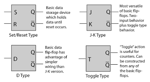
There are basically four different types of flip flops and these are:
>Set-Reset (SR) flip-flop or Latch.
>JK flip-flop.
>D (Data or Delay) flip-flop.
>T (Toggle) flip-flop.

The Set-Reset SR Flip-flop:
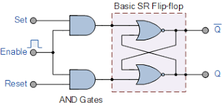
The most basic of all the bistable latches and bistable multivibrators is the set-rest (SR) flip-flop. The basic SR flip-flop is an important bistable circuit because all the other types of flip-flop are built from it. The SR flip-flop is constructed using two cross-coupled digital NAND gates such as the TTL 74LS00, or two cross-coupled digital NOR gates such as the TTL 74LS02.
Working of SR Latch Using NOR Gate
Working of SR Latch Using NAND Gate
What is the JK Flip-flop?
The JK flip-flop is very similar in many ways to the previous SR flip-flop and is probably the most used of all the flip-flop designs. The terms “J” and “K” do not really mean or relate to any special description but where originally used at the time of the flip-flops initial development because these two letters are not used as part of any other digital device. For the JK flip-flop, the “J” is equivalent to Set and the “K” is equivalent to Reset.
The (Data) D-type Flip-flop (Transparent latch)
The D-type flip-flop or Data Latch has only one input referred to as the “D”, or data input, plus a clock input, CLK along with the usual two outputs, Q and Q. The D-type flip-flop transfers its digital data between the input and its outputs, after a delay of one clock pulse and so the “D” part is also referred to as a “delay” input.
Working of D-type Flip-flop (Transparent latch)
Working of Edge-triggered D Flip-flop
The (Toggle) T-type Flip-flop:
The T-type (toggle) flip-flop is a single input bistable, with an operation similar to the D-type above. We saw above with the JK flip-flop configuration, that if J = K = 1 its output would toggle on the application of the next clock cycle. Then the conversion of flip-flops to a Toggle type is simply a matter of connecting the inputs HIGH.
Conversion of Flip-flops:
Flip-flops are the basic building blocks of Sequential Circuits which can be converted from one form to another capable of storing a single bit of data.

What are the Registers?
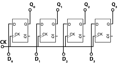
A Register is a collection of flip flops. A flip flop is used to store single bit digital data. For storing a large number of bits, the storage capacity is increased by grouping more than one flip flops.

If we want to store an n-bit word, we have to use an n-bit register containing n number of flip flops.
The register is used to perform different types of operations. For performing the operations, the CPU use these registers. The faded inputs to the system will store into the registers. The result returned by the system will store in the registers. There are the following operations which are performed by the registers:
Fetch:
It is used
>To take the instructions given by the users.
>To fetch the instruction stored into the main memory.
Decode:
The decode operation is used to interpret the instructions. In decode, the operation performed on the instructions is identified by the CPU. In simple words, the decode operation is used to decode the instructions.
Execute:
The execution operation is used to store the result produced by the CPU into the memory. After storing this result, it is displayed on the user screen.
Types of Registers:
There are various types of registers which are as follows:

What is MAR or Memory Address Register?
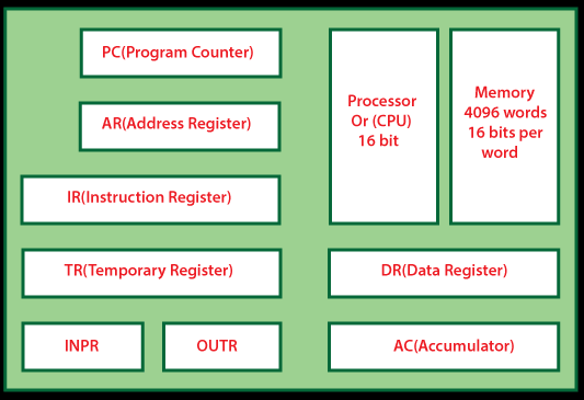
The MAR is a special type of register that contains the memory address of the data and instruction. The main task of the MAR is to access instruction and data from memory in the execution phase. The MAR stores the address of the memory location where the data is to be read or to be stored by the CPU.
What is Program Counter?
The program counter is also called an instruction address register or instruction pointer. The next memory address of the instruction, which is going to be executed after completing the execution of current instruction is contained in the program counter. In simple words, the program counter contains the memory address of the location of the next instruction.
What is the Accumulator Register?
The CPU mostly uses an accumulator register. The accumulator register is used to store the system result. All the results will be stored in the accumulator register when the CPU produces some results after processing.
What is the MDR or Memory Data Register?
Memory Data Register is a part of the computer’s control unit. It contains the data that we want to store in the computer storage or the data fetched from the computer storage. The MDR works as a buffer that contains anything for which the processor is ready to use it. The MDR contains the copied data of the memory for the processor. Firstly the MDR holds the information, and then it goes to the decoder.
The data which is to be read out or written into the address location is contained in the Memory.
What is the Data Register?
The data is written in one direction when it is fetched from memory and placed into the MDR. In write instruction, the data place into the MDR from another CPU register. This CPU register writes the data into the memory. Half of the minimal interface between the computer storage and the microprogram is the memory data address register, and the other half is the memory data register.
Hat is the shift register?
If the register is capable of shifting bits either towards right hand side or towards left hand side is known as shift register. An ‘N’ bit shift register contains ‘N’ flip-flops. Following are the four types of shift registers based on applying inputs and accessing of outputs.
Serial In − Serial Out shift register
Serial In − Parallel Out shift register
Parallel In − Serial Out shift register
Parallel In − Parallel Out shift register
Also read here