What is the SR latch?
What are the SR latch and JK flip flop? An SR latch (Set/Reset) is an asynchronous device: it works independently of control signals and relies only on the state of the S and R inputs. In the image we can see that an SR latch can be created with two NOR gates that have a cross-feedback loop. SR latches can also be made from NAND gates, but the inputs are swapped and negated. In this case, it is sometimes called an SR latch.
When a high input is applied to the Set line of an SR latch, the Q output goes high (and Q low). The feedback mechanism, however, means that the Q output will remain high, even when the S input goes low again. This is how the latch serves as a memory device. Conversely, a high input on the Reset line will drive the Q output low (and Q high), effectively resetting the latch’s “memory”. When both inputs are low, the latch “latches” – it remains in its previously set or reset state.
When both inputs are high at once, however, there is a problem: it is being told to simultaneously produce a high Q and a low Q. This produces a “race condition” within the circuit – whichever flip flop succeeds in changing first will feedback to the other and assert itself. Ideally, both gates are identical and this is “metastable”, and the device will be in an undefined state for an indefinite period. In real life, due to manufacturing methods, one gate will always win, but it’s impossible to tell which it will be for a particular device from an assembly line. The state of S = R = 1 is therefore “illegal” and should never be entered.
| S | R | Q | Q |
| 0 | 0 | Latched | |
| 0 | 1 | 0 | 1 |
| 1 | 0 | 1 | 0 |
| 1 | 1 | Metastable | |
When the device is powered up, a similar condition occurs, because both outputs, Q and Q, are low. Again, the device will quickly exit the metastable state due to differences between the two gates, but it’s impossible to predict which of Q and Q will end up high. To avoid spurious actions, you should always set SR flip-flops to a known initial state before using them – you must not assume that they will initialize to a low state.


Gated SR latch:
In some situations, it may be desirable to dictate when the latch can and cannot latch. The gated SR latch is a simple extension of the SR latch which provides an Enable line which must be driven high before data can be latched. Even though a control line is now required, the SR latch is not synchronous, because the inputs can change the output if the enable line is held high at length. (Note: If a clock is supplied to the control line, the gated SR latch becomes known as an SR flip flop because the output changes only when edge-triggered by the clock.)
When the Enable input is low, then the outputs from the AND gates must also be low, thus the Q and Q outputs remain latched to the previous data. Only when the enable input is high can the state of the latch change, as shown in the truth table. When the enable line is asserted, a gated SR latch is identical in operation to an SR latch.
The Enable line is sometimes a clock signal, but is usually a read or write strobe
| Enable | S | R | Q | Q |
| 0 | 0 | 0 | Latched | |
| 0 | 0 | 1 | Latched | |
| 0 | 1 | 0 | Latched | |
| 0 | 1 | 1 | Latched | |
| 1 | 0 | 0 | Latched | |
| 1 | 0 | 1 | 0 | 1 |
| 1 | 1 | 0 | 1 | 0 |
| 1 | 1 | 1 | Metastable | |

Working of SR Latch using NOR gate
Here is the video lecture of working of SR Latch using NOR gates:
D latch:
The D latch (D for “data”) or transparent latch is a simple extension of the gated SR latch that removes the possibility of invalid input states.
Since the gated SR latch allows us to latch the output without using the S or R inputs, we can remove one of the inputs by driving both the Set and Reset inputs with a complementary driver: we remove one input and automatically make it the inverse of the remaining input.
The D latch outputs the D input whenever the Enable line is high, otherwise the output is whatever the D input was when the Enable input was last high. This is why it is also known as a transparent latch – when enable is asserted, the latch is said to be “transparent” – signals propagate directly through it as if it isn’t there.
| Enable | D | Q | Q |
| 0 | 0 | Latched | |
| 0 | 1 | Latched | |
| 1 | 0 | 0 | 1 |
| 1 | 1 | 1 | 0 |
D latches are often used in I/O ports of integrated circuits and are available as discrete devices, often multiply packaged. An example is the 74HC75, part of the 7400 series of ICs, containing four separate D latches.
JK Flip Flop:
The SR Flip Flop or Set-Reset flip flop has lots of advantages. But it has the following switching problems:
- When Set ‘S’ and Reset ‘R’ inputs are set to 0, this condition is always avoided.
- When the Set or Reset input changes their state while the enable input is 1, the incorrect latching action occurs.
The JK Flip Flop removes these two drawbacks of SR Flip Flop
The JK Flip Flop is one of the most used flip flops in digital circuits. The JK flip flop is a universal flip flop having two inputs ‘J’ and ‘K’. In SR flip flop, the ‘S’ and ‘R’ are the shortened abbreviated letters for Set and Reset, but J and K are not. The J and K are themselves autonomous letters which are chosen to distinguish the flip flop design from other types.
The JK flip flop work in the same way as the SR flip flop work. The JK flip flop has ‘J’ and ‘K’ flip flop instead of ‘S’ and ‘R’. The only difference between JK flip flop and SR flip flop is that when both inputs of SR flip flop is set to 1, the circuit produces the invalid states as outputs, but in case of JK flip flop, there are no invalid states even if both ‘J’ and ‘K’ flip flops are set to 1.
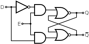
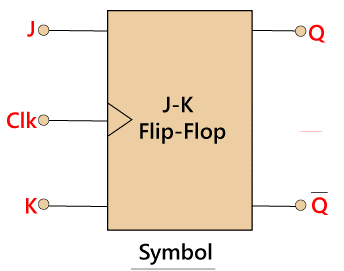
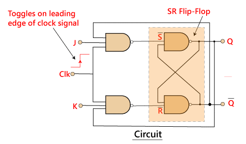
The JK Flip Flop is a gated SR flip-flop having the addition of a clock input circuitry. The invalid or illegal output condition occurs when both of the inputs are set to 1 and are prevented by the addition of a clock input circuit. So, the JK flip-flop has four possible input combinations, i.e., 1, 0, “no change” and “toggle”. The symbol of JK flip flop is the same as SR bistable Latch except for the addition of a clock input.
Block Diagram:
In SR flip flop, both the inputs ‘S’ and ‘R’ are replaced by two inputs J and K. It means the J and K input equates to S and R, respectively.
The two 2-input AND gates are replaced by two 3-input Nand Gates. The third input of each gate is connected to the outputs at Q and Q’. The cross-coupling of the SR flip-flop permits the previous invalid condition of (S = “1”, R = “1”) to be used to produce the “toggle action” as the two inputs are now interlocked.
If the circuit is “set”, the J input is interrupted from the “0” position of Q’ through the lower NAND gate. If the circuit is “RESET”, K input is interrupted from 0 positions of Q through the upper NAND gate. Since Q and Q’ are always different, we can use them to control the input. When both inputs ‘J’ and ‘K’ are set to 1, the JK toggles the flip flop as per the given truth table.
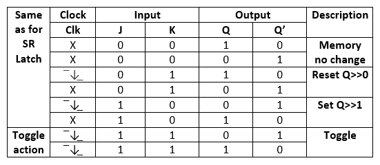
When both of the inputs of JK flip flop are set to 1 and clock input is also pulse “High” then from the SET state to a RESET state, the circuit will be toggled. The JK flip flop work as a T-type toggle flip flop when both of its inputs are set to 1.
The JK flip flop is an improved clocked SR flip flop. But it still suffers from the “race” problem. This problem occurs when the state of the output Q is changed before the clock input’s timing pulse has time to go “Off”. We have to keep short timing plus period (T) for avoiding this period.
Also read here
https://eevibes.com/computing/introduction-to-computing/what-are-the-registers-in-computer-system/