what are the half adder and full adder circuits?
How to design Half adder and Full adder circuits? Adders are the circuits in digital logic design that are used for performing the addition of binary numbers in computers or any computing devices. There are basically two types of adders:
- Half adder
- Full adder
These two circuits can be cascaded to design of adders that can add numbers of ‘n’ number of bits
What is the half adder?
Half adder is a circuit that adds only two bits at a time. These two bits can be 00, 01,10, or 11. The output of half adder consists of two bits: sum and carry. Carry bit is equal to 1 when we add two bits that are 1 and their resultant is of 2 bits. Since 1+1=10. So, here 1 is a carry bit while 0 is the sum bit. The name half adder is derived from full adder. Since a full adder can be designed using two half adders.
The truth table for the half adder is shown below
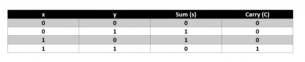
If we look at the “sum” column, we can clearly see that the output of sum=1 only when both inputs are different and sum=0, when both inputs are same. From here it can be concluded that “sum” maps the logic of XOR gate.
Similarly if you notice the output of carry, the output is equal to 1 only when both inputs are equal to 0.This implies that carry can be implemented using AND gate.
The following diagram shows the gate level design of Half adder
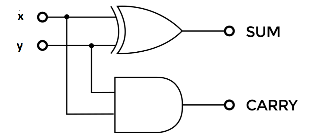
Sum=x⊕y
Carry=xy
What is the full adder?
Full adder is a circuit that adds three input bit to of which are x, y and third one is carry from the proceeding calculations. The output of the full adder is in the form of sum and carry again. Since three bits are involved in process that is why 2^3=8 possible combinations of input are available. The truth table for the full adder is shown below
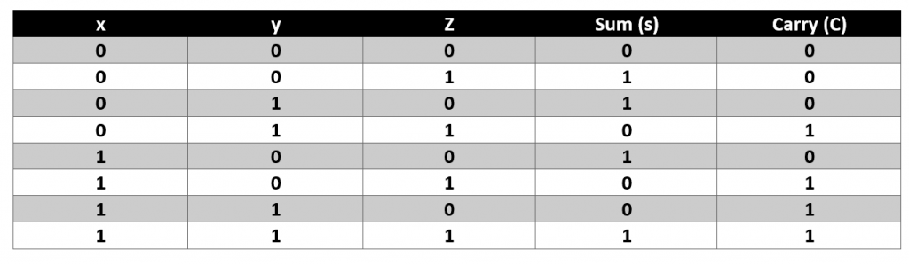
It can be observed again that the output ‘sum’=1 when there are odd number of 1’s. This is the property of logical XOR gate. For carry the expression can be determined using k-map.
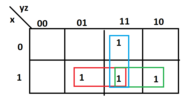
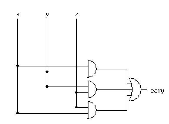
The equation for carry is
carry=xy+yz+zx
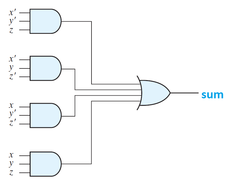
Sum=x⊕y⊕z
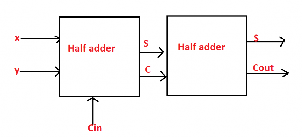
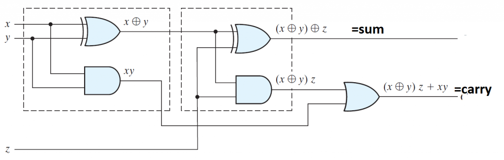
complete full adder circuit is shown below and it can be observed easily that a full adder is composed of two half adders as shown below.
Download the Lab Manual of half adder and full adder circuits.
Download the lab manual of half adder and full adder circuit (lab5)
How to design the half adder, half subtractor, full adder and full subtractor circuits ?
video lecture for half adder and full adder
Also read here
- what are the half subtractor and full subtractor circuits?
- How to design a four bit adder-subtractor circuit?
- What are number systems in computer?
- Discuss the binary counter with parallel load? Explain its working with an example
- how to draw state diagram of sequential circuit?
- How to simplify a Boolean function using Karnaugh map (k-map)?
- What are the flip flops and registers in digital design?
- Define fan-in, fan-out, CMOS and TTL logic levels
- what is the Canonical form representation of Boolean function?