How to Draw State Diagram of Sequential Circuit?
how to draw state diagram of sequential circuit? It is actually the graphical representation of logic circuits. The state diagram is a visual representation of how sequential circuits behave. It clearly depicts the transition of states from one state to the next, as well as the output for a given input. Each current state is represented by a circle in this graphic.
Flip-flops can be graphically represented by a state diagram in addition to graphical symbols, tables, or equations. A state is represented by a circle in this picture, with directed lines (or arcs) connecting the circles indicating the transition between states. Different forms of state diagrams exist, each with its own meanings and characteristics. State diagrams depict finite state machines graphically. They’re solely utilized to figure out how objects behave across the entire system. An example of a state diagram is show below
Each circle has a binary number inside it that represents the condition it represents. Two binary numbers separated by a slash (/) are used to label the directed lines. The input value that triggers the state shift is the first to be labelled. The value of the output is the number after the slash symbol /. The directed line from state 00 to 01, for example, is labelled 1/0, which means that if the sequential circuit is in a current state with a 1 as an input, the following state is 01 with a 0 as an output. If the input is 0 and the current state is 00, it will remain in that state. A circle connected to itself by a directed line shows that no change of condition has occurred.
Although state diagrams are an important and valuable modelling approach, they are not required for every class. The interaction between objects of different classes causes complexity in most systems, as shown in sequence and collaboration diagrams. It’s possible that only a few classes in any system, particularly an information system, will exhibit dynamic behavior, necessitating the use of a state diagram to depict what happens. This is the situation in a system like Wheels, where most classes have objects that only go through a limited number of events and all of the objects react the same way to the same event. In the Wheels case study system, for example, all Customer objects respond to events in the same way, but with varying values: recording details, locating a corresponding Hire object, displaying customer details, and editing customer details. Their reaction to events is independent of their current state. There isn’t much to display on a state diagram for this type of class, which has pretty straightforward behavior. Other types of computer systems, such as process control or communication systems, may feature a lot of classes with exceedingly complex dynamic behavior.
Watch the Video Lecture Here
How to Draw the State Diagram
Analysis of Sequential Circuit using J-K Flip-Flop
Basic Design Steps
A basic example will be used to demonstrate the approaches for creating sequential circuits. Assume we want to create a circuit that fits the following requirements:
1. There is one input, w, and one output, z, in the circuit.
2. All circuit modifications happen on the positive edge of a clock signal.
3. If the input is equal to 1 for two consecutive clock cycles, the output z is equal to 1.
The value of w was one. Otherwise, the value of z is set to zero. As a result, the circuit detects the presence of two or more consecutive 1s on its input w. Circuits with the detection of a specific pattern on its input(s) is referred to as sequence detector.
It is clear from this statement that the output z cannot be exclusively dependent on the w’s current value Consider the values of the w and z signals in order to see what I mean. as indicated in Fig. (b) below.
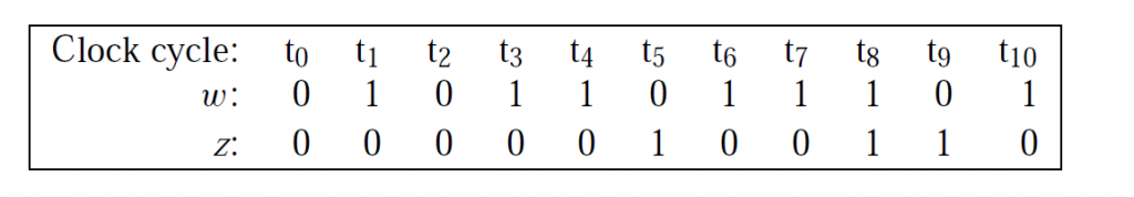
During 11 clock cycles The values of w are chosen at random. The values of z are consistent with our requirements. These input and output value sequences indicate that the outcome for a given input value can be either 0 or 1. For instance, w = 0 z = 0 during clock cycles t2 and t5, but z = 1 during clock cycles t2 and t5. Likewise, w = 1. During t1 and t8, however, z = 0 and z = 1 respectively. This indicates that z is not fixed, only by the current value of w, hence distinct states in the circuit must exist that determine z is the value.
What is the State Diagram?
The first stage in creating a finite state machine is to figure out how many states are required and which transitions between them are possible. This task does not have a set procedure. The machine’s purpose must be carefully considered by the designer. Selecting a starting state, which is the state that the circuit should enter when power is first turned on or when a reset signal is provided, is a good place to start.
Let’s pretend that state A is the beginning point for our case. The circuit does not need to do anything as long as the input w is 0, hence each active clock edge should keep the circuit in state A. When w equals 1, the machine should notice and change to state B. After w has equaled 1, this transition occurs on the next active clock edge.
Because it has not yet seen w = 1 for two consecutive clock cycles in state B, the circuit should hold the value of output z at 0. If w is 0 on the next active clock edge while in state B, the circuit should return to state A. If w = 1 in state B, the circuit should shift to a third state, C, and generate an output z = 1. As long as w = 1 and z = 1 are maintained, the circuit should remain in state C.
The machine should return to state A when w reaches 0. We may conclude that three states are required to create the desired machine because the preceding description addresses all conceivable values of input w that the machine can face in its various states.
We’ll present a more formal process for designing the appropriate sequential circuit now that we’ve defined the various transitions between states in an informal manner. A sequential circuit’s behavior can be explained in a variety of ways.
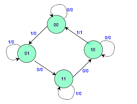
The most basic technique is to utilize a state diagram, which is a graph that represents circuit states as nodes (circles) and transitions between states as directed arcs. The behavior that corresponds to our specification is defined by the state diagram in Figure below.
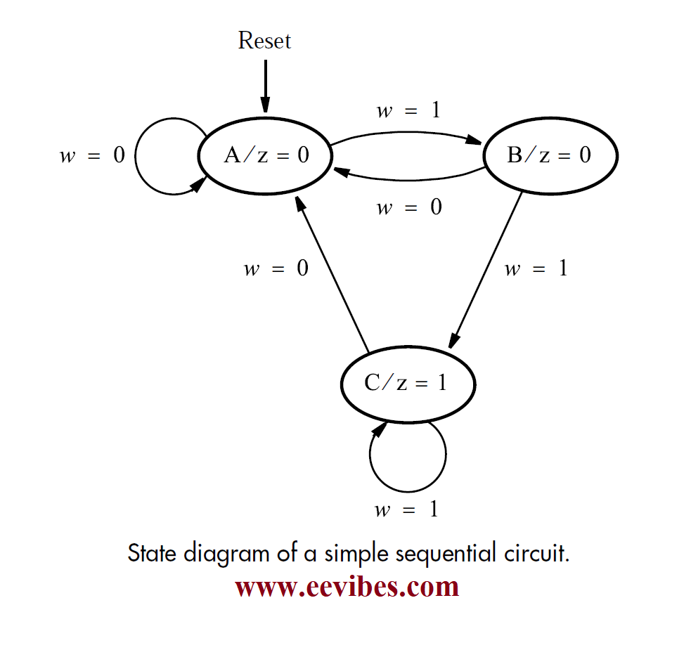
The figure shows nodes for states A, B, and C. Node A reflects the circuit’s initial state, as well as the state it will attain after an input of w = 0. The output z should be 0 in this stage, as shown by A/z=0 in the node. As long as w = 0, which is denoted by an arc with the label w = 0 that begins and terminates at this node, the circuit should remain in state A.
Moving from state A to state B records the first occurrence of w = 1 (after the condition w = 0). An arc originating at A and concluding at B is used to represent this transition on the graph. The input value that initiates the transition is labelled w = 1 on this arc. The output remains at 0 in state B, as represented by B/z=0 in the node.
If w is still equal to 1 at the next active clock edge, the circuit will transition to state C from state B. The output z is equal to 1 in state C. If w remains at 1 for the next clock cycle, the circuit will remain in state C, with z = 1. If w becomes 0 while the circuit is in state B or state C, the next active clock edge will cause the circuit to switch to state A.
We can see in the diagram that the Reset input is used to force the circuit into state A, which is feasible regardless of the circuit’s current state. We could treat Reset as if it were just another circuit input, and depict a transition from each state to the initial state A controlled by Reset. This would unnecessarily complicate the diagram.
Flip-flops are used to implement states in a finite state system. Because most flip-flops have a reset capability, we may presume that the Reset input is used to reset all flip-flops to 0.
What is the State Table?
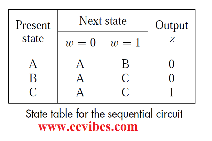
Although the state diagram gives an easy-to-understand description of a sequential circuit’s behavior, it is more convenient to translate the information included in the state diagram into tabular form before proceeding with the circuit’s implementation. The state table for our sequential circuit is shown in Figure below. For varied values of the input signal, the table shows all transitions from each current state to the next one. It’s worth noting that the output z is stated in terms of the current state, or the state in which the circuit is right now. Also, the Reset input was omitted; instead, we assumed that the first state in the table was the initial state.
The design steps that will result in the final circuit are now shown. To demonstrate the fundamental design concepts, we first go through the traditional procedure of doing each design stage manually. A description of automated design processes using modern computer assisted design (CAD) tools follows.
State Assignment
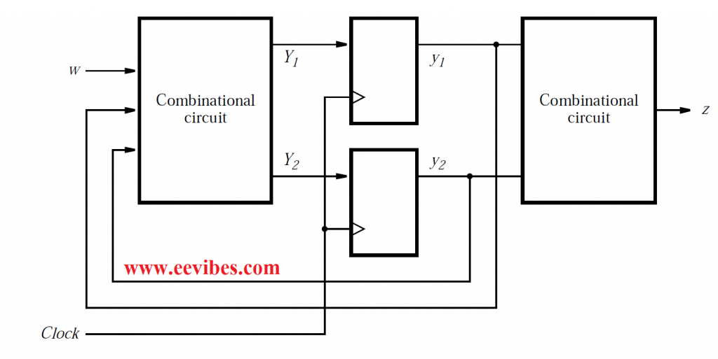
The three states are defined in the state table in Figure shown above by the letters A, B, and C. Each state is represented by a specific valuation (combination of values) of state variables when implemented in a logic circuit. A flip-flop can be used to implement each state variable. Because three states must be achieved, only two state variables are required. Let’s call these two variables y1 and y2.
We can now apply the following general block diagram to our example (c), as shown in Figure (d), to show the structure of the circuit that implements the required finite state machine.
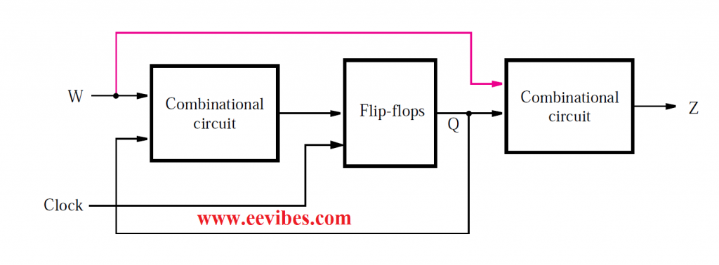
The state variables are represented by two flip-flops. The type of flip-flops to be used is not stated in the illustration; this issue is addressed in the next subsection. According to the specifications in Figures of state diagram and state table, the output z is solely determined by the circuit’s current state.
As seen in Fig. (d), z is just a function of y1 and y2, indicating that our design is Moore type. We need to create a combinational circuit that takes the input signals y1 and y2 and outputs the proper output signal z for all conceivable input values.
The y1 and y2 signals are also transmitted back to the combinational circuit, which decides the FSM’s next state. The principal input signal w is also used in this circuit. Two signals, Y1 and Y2, are outputs that are utilized to set the state of the flip-flops. Each active edge of the clock causes the flip-flops to change state to the current values of Y1 and Y2. As a result, the next-state variables are Y1 and Y2, while the present-state variables are y1 and y2. We need to create a combinational circuit with the inputs w, y1, and y2, so that the outputs Y1 and Y2 cause the machine to shift to the next state that meets our requirements for all values of these inputs. The truth table that describes this circuit, as well as the circuit that yields z, is the next step in the design process.
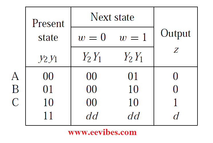
We assign a specific valuation of variables y1 and y2 to each state to construct the desired truth table. Fig. (e) shows one possible assignment, with the states A, B, and C represented by y2y1 = 00, 01, and 10, respectively. In this situation, the fourth valuation, y2y1 = 11, is unnecessary.
A state-assigned table is the type of table illustrated in Figure 8.6. With the inputs y1 and y2, this table can be used directly as a truth table for the output z. Although the table does not appear to be a normal truth table for the next-state functions Y1 and Y2, because there are two separate columns in the table for each value of w, it is obvious that the table contains all of the information that defines the next-state functions in terms of input w, y1, and y2 valuations.
Choice of flip flops and derivation of next state and output expressions
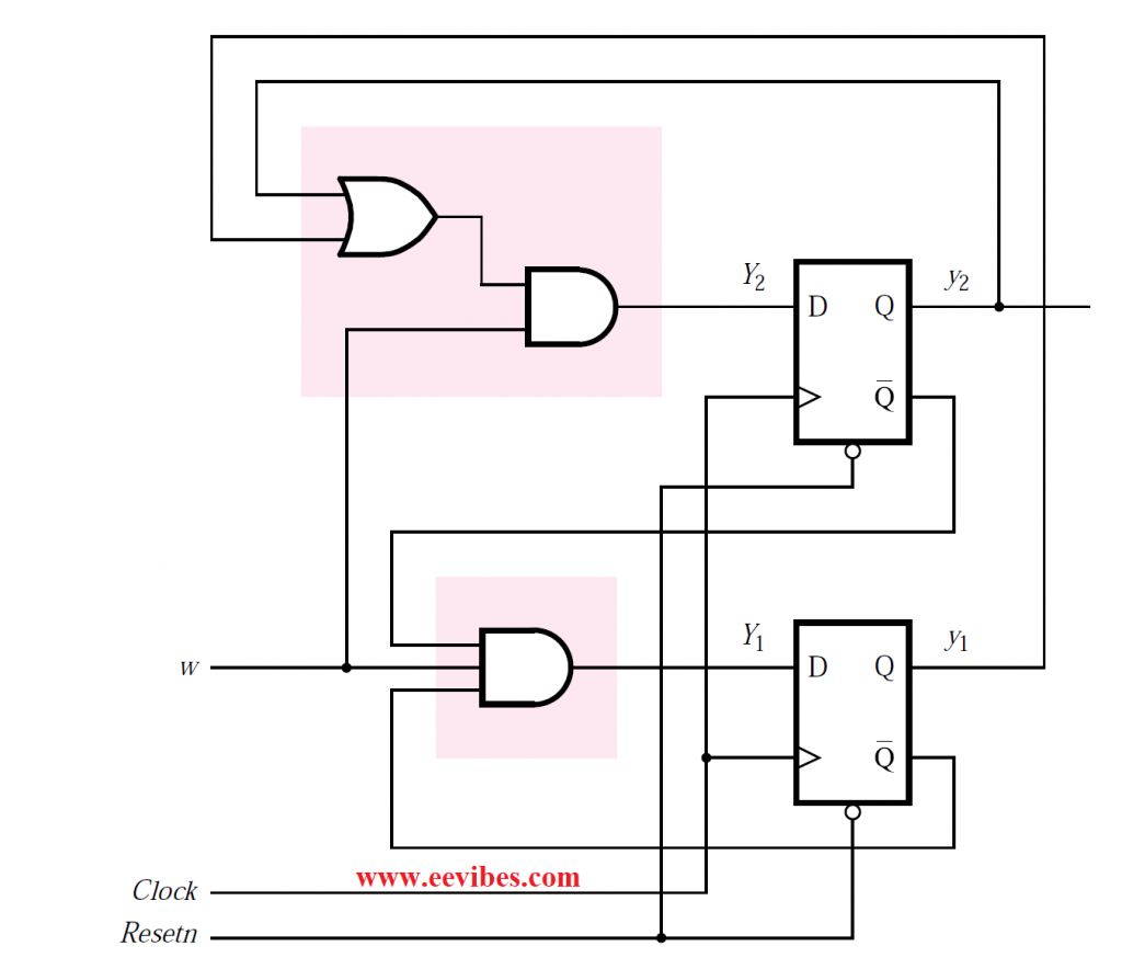
The logical expressions for the next-state and output functions can be derived from the state-assigned table in Fig. (e). However, we must first choose the sort of flip-flops to be used in the circuit. The simplest option is to utilize D-type flip-flops, because the values of Y1 and Y2 are simply clocked into the flip-flops and become the new values of y1 and y2. In other words, if the flip-flops’ inputs are labelled D1 and D2, these signals are labelled Y1 and Y2. Fig. (d) shows exactly how D-type flip-flops are used in this application. The link between the next-state variable and the inputs to a flip-flop is not as easy for other sorts of flip-flops, such as JK type.
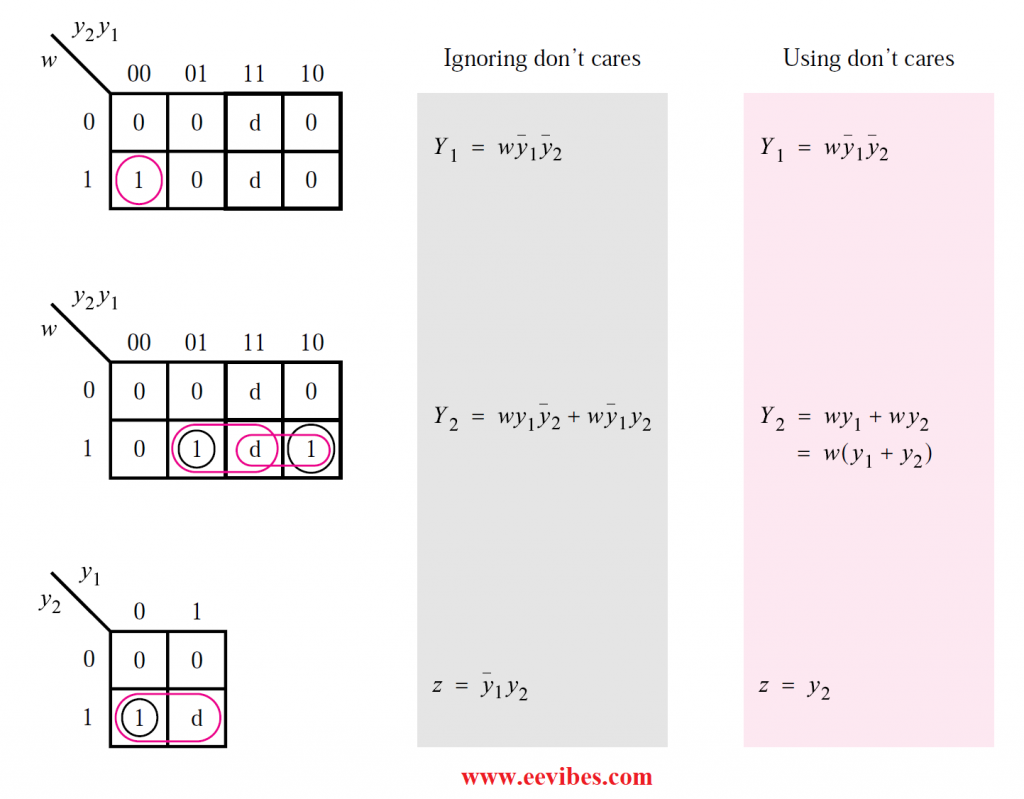
Fig. (f) shows how to derive the appropriate logic expressions. We use Karnaugh maps to make it simple for the reader to check the expressions’ validity. Remember that we only needed three of the four potential binary valuations to express the states in Fig. (e). Because the circuit is confined to travel only within states A, B, and C, the fourth valuation, y2y1 = 11, should never occur in the circuit; consequently, we can regard this valuation as a don’t-care condition. In the Karnaugh maps, the resulting don’t-care squares are marked by d’s. We get the following result by using the don’t care conditions to simplify the expressions.
Y1 = wy1’y2′
Y2 = w(y1 + y2)
z = y2
The resulting phrases are slightly more complex if we don’t use don’t cares; they are represented in the gray-shaded section of Fig.(f). Because D1 = Y1 and D2 = Y2, Fig. (g) depicts the logic circuit that corresponds to the foregoing formulas. It’s worth noting that the circuit has a clock signal and an active-low reset capability. The clear input on the flip-flops can be connected to an external Reset n signal, as illustrated in the image, to force the circuit into a known state. When the signal Reset n = 0 is applied to the circuit, both flip-flops are reset to 0, putting the FSM in the state y2y1 = 00.
Timing Diagram
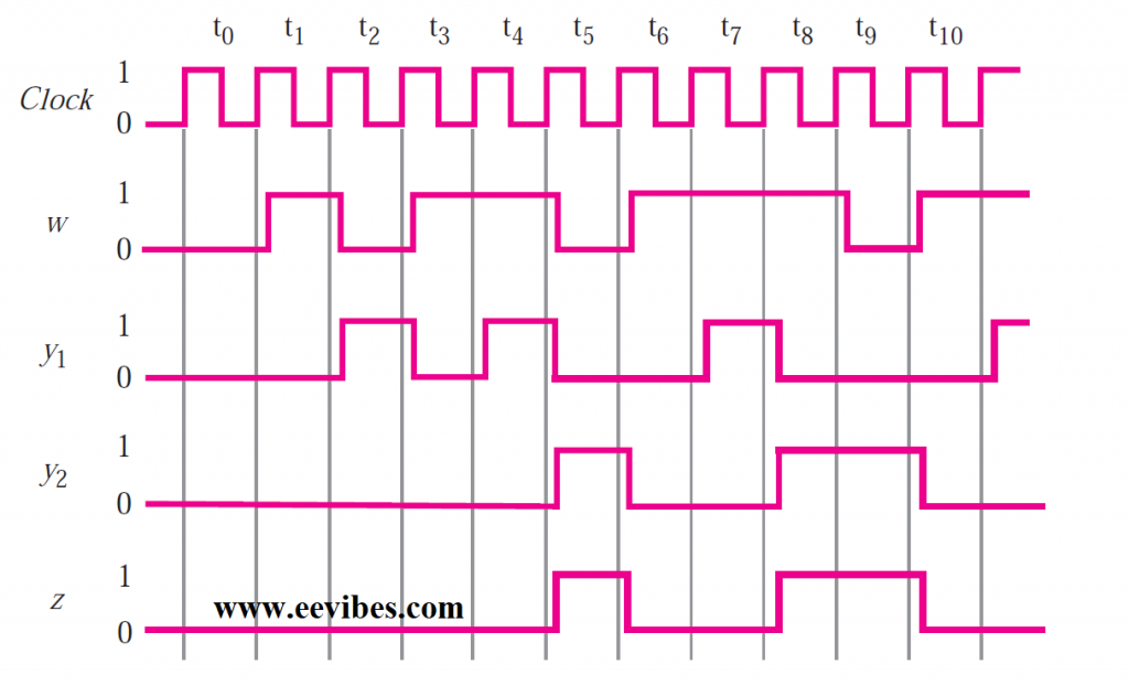
Consider the timing diagram in Fig. (h) to fully comprehend the behavior of the circuit in Fig. (g). The signal waveforms in the figure match to the value sequences in Fig.(b).
Because we’re utilizing positive-edge-triggered flip-flops, all signal changes happen right after the clock’s positive edge. The propagation delays through the flip-flops determine the amount of delay from the clock edge. It’s worth noting that the input signal w changes slightly following the clock’s active edge. This is a reasonable assumption because in a normal digital system, an input like w would be nothing more than an output of another circuit synchronized by the same clock.
Even if w changes slightly after the active clock edge, and thus the value of w is equal to 1 (or 0) for virtually the entire clock cycle, no change in the circuit occurs until the positive edge triggers the flip-flops to change their state at the start of the following clock cycle. If the circuit is to reach state C and generate the output z = 1, the value of w must be equal to 1 for two clock cycles.
5.6 A sequential circuit with two D flip-flops A and B, two inputs, x and y ; and one output z is specified by the following next-state and output equations:
A(t + 1) = xy’+ xB
B(t + 1) = xA + xB’
z = A
(a) Draw the logic diagram of the circuit.
(b) List the state table for the sequential circuit.
(c) Draw the corresponding state diagram.
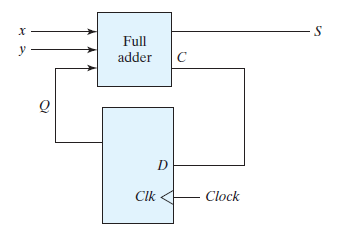
5.7 A sequential circuit has one flip-flop Q, two inputs x and y, and one output S . It consists of a full-adder circuit connected to a D flip-flop, as shown in Fig. P5.7 . Derive the state table and state diagram of the sequential circuit.
What is the Gray Code?
The Gray Code, also known as reflected binary code, is a series of binary number systems. The initial N/2 values are compared to the last N/2 values in reverse order, which is why this code is called reflected binary code. Two successive values are separated by one bit of binary digits in this coding. In the general sequence of hardware-generated binary numerals, grey codes are employed. When transitioning from one number to the next, certain numbers might generate ambiguity or problems. When the transition between numbers is complete, this code simply addresses the problem by modifying only one bit. Gray code assesses the nature of binary code, or data made up of on and off signs, which are frequently represented by ones and zeros. Gray code, developed by Bell Labs scientists, has been used to investigate binary communications clarity and error correction. Gray code, also known as reflected binary code, is a type of binary coding.
Gray code essentially sophisticates and clarifies binary outcomes. Physical switches for binary code are discussed as part of this procedure; nevertheless, experts warn that physical switches may not synchronize perfectly. Other issues include signal noise, which can result in transmission issues due to lost binary bits or integers.
Gray code does this by looking at one switch or piece of binary code at a time, and going through binary code slowly looking for consistency. Applications for digital terrestrial TV transmissions and cable-delivered digital signals are two common examples. Because it is not dependent on the value of the digit indicated by the location, the grey code is a very light weighted code. This code is also known as a cyclic variable code since the transition from one value to the next only changes one bit. Because it is not dependent on the value of the digit indicated by the location, the grey code is a very light weighted code. This code is also known as a cyclic variable code since the transition from one value to the next only changes one bit.
To generate the Gray code of a number, the prefix and reflect methods are applied recursively. To generate grey code, follow these steps:
- The amount of bits required to represent a number is determined.
- Then we look for the code for zero, which is 0000, which is the same as binary.
- Now we’ll replace the most significant portion of the prior code, which is 0000.
- We carry doing this procedure in secret until all of the codes are unidentifiable.
- If changing the most significant bit yields the same result as changing the second most significant bit, the third most significant bit will be altered, and so on.
Gray code is a type of non-weighted code that is a subset of unit-distance code. The bit pattern for two consecutive numbers differs in only one-bit location in unit-distance code.
For example, these codes are sometimes known as cyclic codes.
- The decimal number 5 is represented by the grey symbol 0 1 1 1
- 0 1 0 1 is the grey cod for the decimal number 6.
The only difference between these two codes is one-bit location.
Because of this feature, this code is widely employed in shaft encoders.
- Gray code is code that has been reflected.
- The following property can be used to create grey code.
i)1 Bit Gray Code has two code words, 0 and 1, which represent decimal numbers 0 and 1.
- ii) An n>2 (n-bit) Gary Code will have the leading 0 appended to the first 2n-1 Gray Codes of (n-1) bit written.
iii) The final 2n-1 Gray Code will be the reverse order Gray Code words of a (n-1) bit Gray Code.
The table below will help you to understand the concept better .
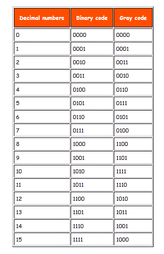
The comparable grey coding of decimal numbers can be found in this table. There are various procedures that will help you comprehend how codes are constructed. In the case of grey code, each step will modify one bit from the preceding one. One thing to remember is that bit changes always happen on the right side, from the L.S.B to the M.S.B. The first three bits remain constant, i.e. 000, but the fourth bit shifts from 0 to 1. We know that the only binary digit combinations are 0 and 1, therefore keeping the first three bits constant eliminates the possibility of a 4th bit combination for decimal 0 and 1.
Click below to read more articles