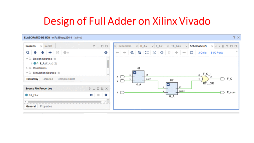
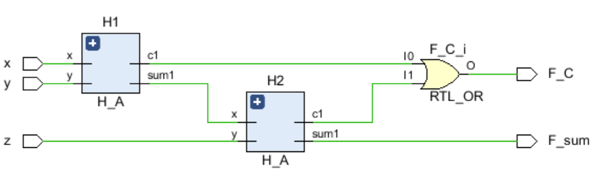
In this article, I will explain how to write a verilog code for a Full Adder Circuit on Vivado sosftware by using two Half Adders. First of all, you need the block diagram that actually depicts the relation of half adder and full adder circuit. The block diagram is shown below:
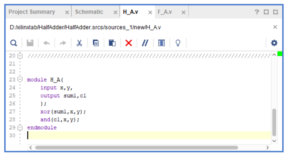
Verilog Code for Half Adder
module H_A(input x,y,output sum1,c1);
xor(sum1,x,y);
and(c1,x,y);
endmodule
Verilog Code for Full Adder
module F_A(input x,y,z,output F_sum, F_C);
wire sum1,c1,c2;
H_A H1(x,y,sum1,c1);
H_A H2(sum1,z,F_sum,c2);
or(F_C,c1,c2);
endmodule
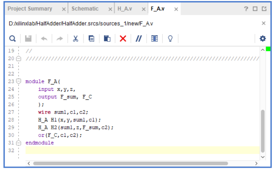
In thr above code of full adder, it can be seen that I have created instances of previously defined half adder.
Test Bench Code for Full Adder in Xilinx Vivado
timescale 1ns/1ps
module test_F_A;
// Inputs
reg x, y, z;
// Outputs
wire F_sum, F_C;
// Instantiate the Unit Under Test (UUT)
F_A uut (
.x(x),
.y(y),
.z(z),
.F_sum(F_sum),
.F_C(F_C)
);
initial begin
// Monitor the signals
$monitor(“Time=%0t x=%b y=%b z=%b | Sum=%b Carry=%b”,
$time, x, y, z, F_sum, F_C);
// Apply all input combinations
x = 0; y = 0; z = 0; #10;
x = 0; y = 0; z = 1; #10;
x = 0; y = 1; z = 0; #10;
x = 0; y = 1; z = 1; #10;
x = 1; y = 0; z = 0; #10;
x = 1; y = 0; z = 1; #10;
x = 1; y = 1; z = 0; #10;
x = 1; y = 1; z = 1; #10;
$finish;
end
endmodule
Description of Testbench
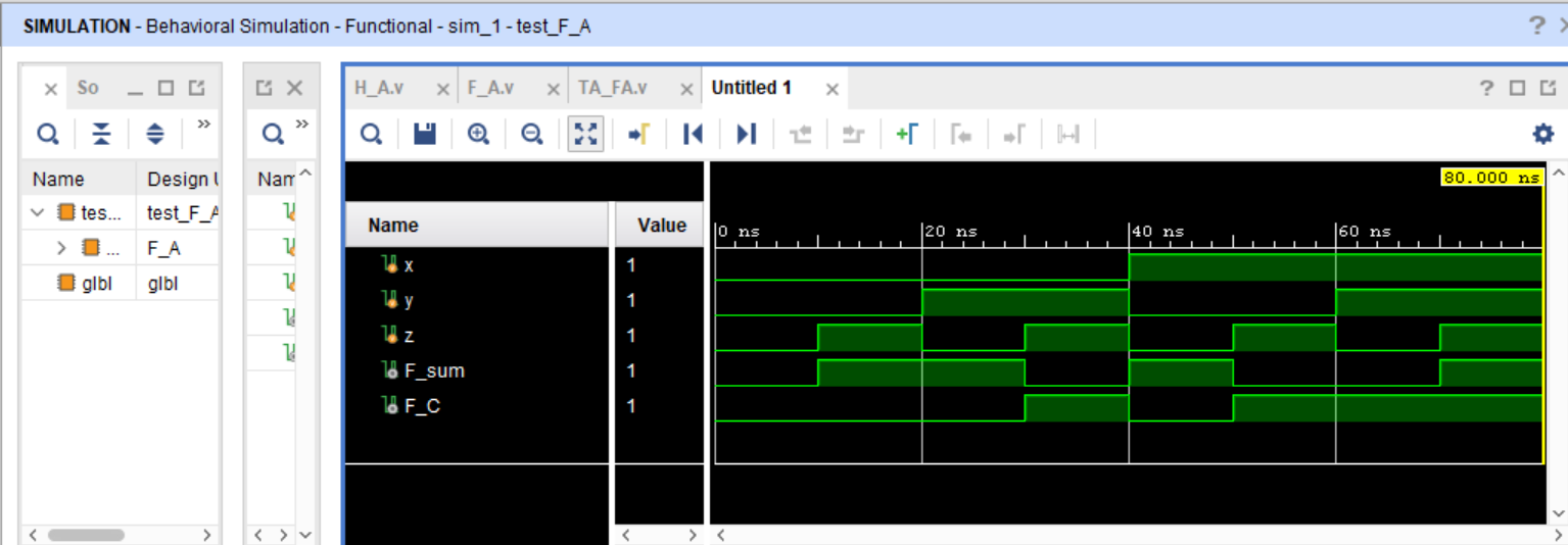
The testbench for the full adder is designed to verify the correct operation of the F_A module. It declares input signals (x, y, z) as registers and output signals (F_sum, F_C) as wires. The full adder is instantiated inside the testbench, and all possible input combinations (000 to 111) are applied sequentially with a fixed time delay. The $monitor command is used to continuously display the inputs and corresponding output values during simulation.
-
"Time=%0t x=%b y=%b z=%b | Sum=%b Carry=%b"
This is the format string. It tells Verilog how to display the values.-
%0t→ prints simulation time -
%b→ prints the value in binary format
-
-
$time
Prints the current simulation time. -
x, y, z
These are the inputs to your full adder. -
F_sum, F_C
These are the outputs of the full adder.
This testbench does not contain any hardware; instead, it provides a controlled environment to test the functionality, timing, and correctness of the full adder design.
Here is the complete video tutorial for this