Introduction
What are the sequential programmable devices? Digital systems are designed with flip‐flops and gates. Because the combinational PLD is made up entirely of gates, external flip-flops must be included when they are employed in the design. Gates and flip-flops are examples of the sequentially programmable devices. As a result, the device may be designed to carry out a wide range of sequential circuit functions. Commercially available sequential programmable devices come in a variety of shapes and sizes, each with its own set of functions. Within each kind, there are vendor-specific variants. These devices’ internal logic is too complicated to be shown here, As a result, we’ll outline three major types of sequential programmable devices:
1. Sequential (simple) programmable logic device (SPLD):
A simple programmable logic device (SPLD) is a less complex programmable logic device than a complex programmable logic device (CPLD). In SPLD, each section is referred to as a Microcell.
2. Complex programmable logic device (CPLD):
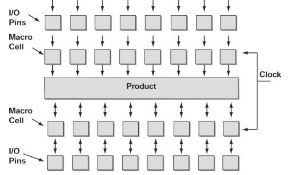
A CPLD is a single integrated circuit that contains a collection of independent PLDs. Typically, each PLD has about 8 to 16 macrocells. The programmability of a CPLD is divided into two levels:
- Each PLD block is unique.
- Interconnections among the PLDs.
A three-state buffer drives each I/O pin, which can be designed to operate as both input and output. If a macrocell has any unused product terms, other macrocells nearby can use them. The macrocell flip-flop can be programmed to operate as a D, JK, or T flip-flop in specific instances.
3. Field‐programmable gate array (FPGA):
The FGPA is a VLSI circuit that may be programmed at the user’s location. There are hundreds or thousands of logic blocks in it. It consists of:
- Programmable input and output blocks.
- Programmable interconnection.
Lookup tables, multiplexers, gates, and flip-flops make up a typical FPGA logic block. A lookup table is a truth table stored in SRAM that offers the logic blocks combinational circuit functions.
what is the Sequential (simple) programmable logic device (SPLD)?
The most basic PLD devices have programmable array logic (PAL) and programmable logic array (PLA) designs. Both of these devices are simple programmable logic devices, which are a type of logic device (SPLDs). The development of two logic gate array structures is the foundation of PLA device architectures. The first array contains Boolean ANDs, whereas the second contains Boolean ORs. These arrays can be used to build a sum of products that implement the appropriate Boolean logic equations when used together. These devices contain input and output blocks, as well as a few configurable internal signal routing channels that can provide feedback on the output signal.
A PAL device has a fixed OR plane, whereas PLA devices allow both the AND and OR planes to be programmed. The trade-off between these two architectures is speed over logic flexibility.
Both of these device topologies, however, are relatively quick, with propagation delays (often referred to as Tpd) in the nanosecond range.
Both PAL and PLA devices are tiny, with pin counts ranging from 16 to 28 and logic cells ranging from 8 to 24. EPROM and EEPROM are the configuration technologies employed in these devices. The 22V10 is a popular PAL architectural example.
To distinguish it from the complicated PLD, the sequential PLD is sometimes referred to as a simple PLD. In addition to the AND-OR array, the SPLD features flip-flops within the integrated circuit chip. A PAL or PLA is modified by the addition of a register made up of many flip-flops. The outputs of the circuit can come from the OR gates or the outputs of the flip-flops.
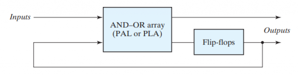
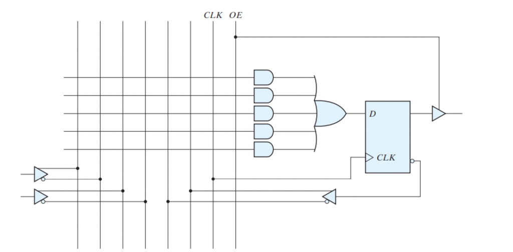
There are additional programmable connections available to include the flip-flop outputs in the AND array’s product terms. The flip-flops could be of the D or JK variety. The combinational PAL with D flip-flops is the most common configuration in an SPLD. As it includes flip-flops in addition to the AND-OR array, a PAL with flip-flops is referred to as a registered PAL. A macrocell is a circuit that contains a sum of products combinational logic function and an optional flip-flop in each segment of an SPLD. The AND-OR array is identical to the combinational PAL. An edge-triggered D flip-flop coupled to a common clock input drives the output, which changes state on a clock edge. A three-state buffer (or inverter) is attached to the flip-flop, which is controlled by an output-enable OE as shown in the figure. The flip-flop’s output is routed back into one of the gates of programmable AND gates inputs to provide the current state condition for the sequential circuit. Within one IC package, a typical SPLD contains 8 to 10 macrocells. All three state buffers are connected to the common CLK input, and the flip-flops are connected to it.
Also read here
https://eevibes.com/digital-logic-design/what-are-the-gate-delays-how-to-reduce-the-gate-delays/