What are the gate delays?
What are the gate delays? In electronics, digital circuits and digital electronics, a term named ‘the Propagation delay, or Gate delay’ is used. “Real gates don’t switch instantaneously. There is a latency between when the input changes and the output changes. We call that latency the propagation delay or gate delay.”
In Verilog terms, logic gates can have propagation delays ranging from more than 10ns down to the picosecond range, depending on the technology being used. The propagation delay of a gate is specified in terms of time units and by the symbol #. The numbers associated with time delays in Verilog are dimensionless. The association of a time unit with physical time is made with the `timescale compiler directive. An example of a timescale directive is as follows: `timescale 1ns/100ps.
Explanation:
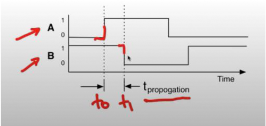
There’s sometime between when we change the input to a circuit and it’s output change and these are due to the fact that our gates are built out of real materials and electrons can’t propagate through these circuits instantaneously if we have an example circuit like this inverter its input A may change at one time what we call t=0, and it’s output B would change at a later time but we will call t1 and the difference between these two is the propagation delay or T propagation representing some finite amount of time between when the input changes and the output changes. It turns out in the general case propagation delay is very complicated and there’s a number of reasons for this. First, the delay from one input say X to the output can be different based on whether X transitions from 0 to 1 then from when X transitions from 1 to 0.
Furthermore, the delay from one input X to the output Z could differ from the delay from Y to Z. In addition, the more things that are attach to this circuit change the amount of time it takes that circuit changes the amount of time it takes that the circuit to switch so if this NAND gate is only driving a single inverter it might switch quickly but as there is attached additional circuits to the output of this NAND gate it will take longer to switch and finally if there are long wires that connect this circuit to another circuit those long wires can add capacitance and resistance which again cause this NAND gate to take longer to switch so computing propagation delay in the general cause is relatively complicated but for the purpose of this class, we can consider propagation delay to be a much simpler thing and we are going to make two simplifying assumptions to make our work easier first is that for a given gate we are gonna say the delay is the constant from any input to the output and second we are going to ignore fan-out and wire delay.
So let’s consider a more complicated example of computing propagation delay in this picture, full adder is shown with inputs X,Y and carry-in and it’s output sum and carry-out and we are gonna make assumptions about the propagation delays of the individual gates and these are arbitrary numbers but ones just to make the example relatively clean so we are going to assume that OR gate take 10 picoseconds or AND gate have a 20 picosecond propagation delay and our XOR gates because they are a little more complicated have a delay of 40 picoseconds.
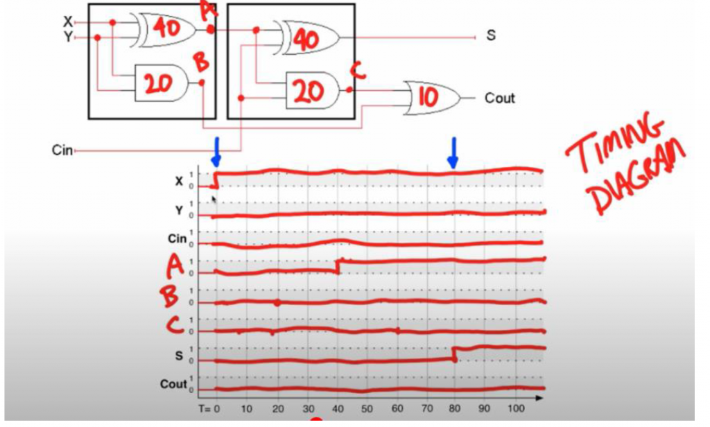
So it is shown here on bottom a timing diagram which is a way to show the value of multiple cycles evolving over time and so on the X-axis. Here it can be seen that time is increasing to the right and initially X,Y and Cin all have the value 0 and at time 0. Now change X to the value 1 and then hold that value for the rest of the example with Y and Cin I am just gonna hold their values at 0 throughout the whole example so we want to see what effect this change has on the circuit and so on we know X is connected to this XOR gate and I am going to call the output of the this XOR gate A and so we know A is not gonna change for at least 40 picoseconds that up until time 400 we know ADE’s value is not going to change that when X and Y, we are both 0 the output of the XOR gate is 0 and it is going to stay that way until 40 picoseconds after A changes then at that point the effective X change can be seen on this output so that now X is 1 and Y is 0 so the output of this XOR gate is 1 and since X and Y do not change again we are gonna hold this output value for the rest of the example similarly the output of the AND gate. I am gonna call B and we know it is not change for 20 picoseconds.
After 20 picoseconds the change in X could affect B but in this case X is 1 and Y is 0, so the output of this AND gate stays 0 the output of this XOR gate is the value of sum and we know that it can not change before A changes, so for the first 40 picoseconds it does not change then when A changes it’s propagation delay of this XOR gate is going to be another 40 picoseconds up to 80 and at that point , the output of the XOR gate could affect S.
So let’s compute the new value of this XOR gate A has the value 1 and carry-in has the value of 0. So one XOR with 0 is 1, so the value does change so let’s look at the output of this AND gate will call that C. C’s inputs are A and carry-in which initially were both 0, so the end of those things is 0 and let’s going to hold it’s value for quite sometime until A changes, we know that C is not going to change it’s value and it is going to be another 20 picoseconds after A changes, so we know it is going to hold it’s value at least until times 60 and again A is now 1 and carry-in is still 0.
So the end of 1 and 0 remains 0, so this signal is gonna stay 0 for the whole example and finally carry-out is the or of C and B well C and B are both 0 for the whole example and so carry-out is going to be 0 for the whole example. So what we see, we see that by changing X at time 0 we have a change in S at time 80 but carry-out doesn’t change at all for this change in X, so in general when we consider one of these propagation delay problems, we are concerned about finding the longest past through a circuit and may be that’s from any input to any output and the way we do this is we compute for every particular input the longest path from it to the output and so we will do that for X to S, so if X changes at time 0, we know that it’s output is going to change at time 40, that’s the earliest that it’s output could change and similarly, it could affect the output of the AND gate at time 20, that means that the output of this XOR gate or S is going to be 40 time units after that change because the other input to that XOR gate is Cin, which is not changing in this analysis and so we can see that there is one path from X to S and it has time 80 time units.
So we have delay of eighty on that path if we look at other output Cout, we see that there is two paths that lead from X to that output and one of those we already know that the bottom input of the OR gate arrives 20 picoseconds after X changes the top input changes while it’s input changes 40 picoseconds after X changes and therefore it’s output is gonna change 60 picoseconds and since we are looking for the longest path we are going to consider when both outputs are stable which is 60 picoseconds.
After X changes and so the output Cout is gonna stabilize 20 picoseconds after X changes, so X to Cout is going to be 70 and it turns out that the circuit is symmetric with respect to X with Y and so we are gonna see a similar 80 and 70 picoseconds latency from Y to S and from Y to Cout but for Cin it’s a little difference when the input Cin changes at time 0 that’s gonna change the output of this AND gate at this time 20 and the output of the XOR gate at time 40, so the latency between Cin and S is 40 picoseconds and then there’s another 10 picoseconds after this 20. So the delay from Cin to Cout is 30, so in this way we are going to look for every path from the input and find the longest to the output.
Steps to reduce the gate/propagation delay:
According to the experts, following few steps are used to reduce gate delay.
1. Minimize no. of transistors through the propagation path.
2. Minimize capacitive (C) effect through propagation path, since cap. ‘C’ makes delay=R*C. This ‘RC’ delay slows down/degrades the signal propagated through the path.
3. By limiting the ‘transitions’ through ‘layers’ as much as possible.
4. By reducing the capacitive effects at the output.
Also read here
What is the meaning of memory decoding in digital circuitry?