What is the meaning of memory decoding in digital circuitry?
What is the meaning of memory decoding in digital circuitry? A digital circuitry is such a circuit which that just process the signal having two states either zero or one. Various Boolean logics are performed with the help of transistors on a circuit.
A hub for memory called memory units in a digital circuit, requires some storage components along with a decoded circuit which helps to specifies the memory on indication of the input.
Memory Decoding Process:
When there is a need to access memory in a digital circuitry, a binary addresses of the wanted memory locations are generated. The memory units with the help of address, find the data which is requested. This is a process of various steps, where a lot of addresses are used to locate the exact memory. In digital electronics, the very initial step is to identify the memory location which is required. The very next step is to locate some more bits of the addresses as there are various chips on the circuit. From inside, the chip is sorted in number of rows and columns in a circuitry. The location of the memory where the rows and columns intersect is the required one. Hence, we used the whole address then split it into pieces. And with the help of each piece, we narrowed the location of the memory. This is known as memory decoding in a circuitry.
A memory cell:
A typical memory cell contains an input, select, read/write and an output. A cell is basically an electronic component which have almost four to six transistors.
A memory cell can store binary signals in various groups called as bits. The other name for bits is the words. A one byte is equal to 8 bits, and one word equals 2 bytes. The data input and output lines held the communication among the memory and its operation, selection lines, and write or read control. This all collectively helps to determine the transfer of the information in bits or words. Every word held a number in the memory called as address which ranges from 0 to 2k-1. Here, k is the number of addresses lines.
Explanation:
The storage component of a cell is designed by a SR latch mechanism with linked gates to form a latch D. The select input of a memory cell permits the cell to read or write and the read/write input regulates the cell operation when it is selected. A ‘1’ in the read/write input provides the read operation by fanned a path from the latch to output. A ‘0’ in the read/write input gives the operation to write by forming a mechanism for a path from the input to the latch.
Construction:
The construction of a RAM contains four bits each and 16 binary cells in total. The small blocks mentioned BC shows the binary cell with three inputs and one output. A memory having four words wants two addresses lines. The two address of the inputs pass through a 2 4 decoded circuit to choose anyone of the four words. The decoder is associated with a memory input.
0 and 1 logic levels
When 0 is enabled as a memory, the decoded circuit output is 0 and none of the words of a memory are chosen. With 1 is selected as a memory, one of the four memory words is designated and the two address lines gets the value.
Read/Write Operation:
Once the word gets sorted, the input of the read/write shows the operation of the cell. While reading, all the four bits go through the OR gates to the terminals of the output.
During writing performance, the data at the input got transmitted to the four binary cells of the word chosen. The cells that the user didn’t select becomes incapacitated and the binary values remains the same and experienced no change.
When the input of the memory is chosen it goes into the decoded circuit and becomes equal to 0, And none of the words are selected and the values of the cell remains unchanged no matter what is the value of the read/write input of the memory cell.
Decoded Address Memory:
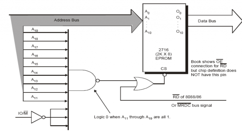
In the commercially random access memory, there is a vacant space for thousands of words of the memory addresses. Each one of the word of the memory ranges from 1 to 64 bits. The direct expansion of configuration of the large number of memory addresses capacity is logically constructed. A memory having 2^k number of words requires the k memory addresses lines with n number of bits per word of the memory. The decoder is of the k*2^k memory addresses. Every one of the decoded address output choose a single word having n number of bits for further reading or writing.
In this operating mechanism, the address line represents the data input which is code and the outputs are basically the correspondent word signal either high or low. Every memory located chip is with an input called as chip select which is inserted in PCs or microprocessor units. Specified memory chip is required to select. Typically, a logic one on the chip input selects the memory coded device whereas a logic zero on the input refrain the memory coded address. Thus, by either selecting or not selecting, a single chip is operated at one time. This way, we can select the right memory address coded device for a specific memory address location. The advantage of memory decoded address is that when we choose a particular memory coded address, the memory location address shows up in only one of the chips correspondently
Coincident Decoding:
A decoder having some k number of inputs have outputs of 2^k. This sort of decoder requires 2^k AND gates and k inputs should be at each gate. The final number of gates and the inputs per gate could be lowered by inserting two decoders in a two dimensional scheme.
One decoder is meant for the selection of row and the other one is for the column selection in a bi-dimensional matrix scheme. In this, two k/2inputs are basically used rather than one k inputs.
Example:
For instance, in the selection scheme for 1K word of memory, rather than using a 10 x 1,024 decoder, the preference should be two 5 x 32 decoders. In a single decoder, we required 1,024 AND gates with ten inputs in each gate. In case of two decoders, we would require 64 AND gates with five inputs at each one of the gate. The very first five most significant bits gets the input X and the least significant bits which are five will go to the input Y. Every word in the memory array is selected as the coincidence of one X line and the one Y input. Hence, single word in the memory is choosen by the coincidence factor between 1 of 32 rows and 1 out of the 32 columns for almost a total of 1,024 words. The intersection of the certain row and column gives the required word. All the bits of the required word are then proceeded to reading and writing.
Address Multiplexing:
Six transistors are there in static random access memory (SRAM). The high density memory cells are produced when the transistors are reduced. The dynamic random access memory (DRAM) has a capacitor too which helps in refreshing the memory by recharging of the cell. Because of this, DRAM has more capacity of storing the memory than SRAM. The cost for storing the data in SRAM is more than the DRAM. The DRAM has less power requirements.
Mostly, DRAM have a size of 1 word bit, so various chips are required. The main reason is the larger capacitive ability, the decoding of all the bits of DRAM is processed in a two dimensional array and if there are larger memory data in a cell, then multiple arrays are required. For the number of pins in the Integrated circuits needs to be lowered, then designers make use of the address multiplexing wherein the address of the input pins can fit in the address components of the cell.
An array having two dimensions, the address is split in two parts for different set of times. The row addresses come first and then the column addresses. As, the similar pin set is used for all the two parts of the address of the memory, the overall size of the package is decreased purposely.
Example:
A 64K word memory is required for multiplexing. The address of the memory contains two dimensional array of the cells which are arranged into 256 rows and the 256 columns. Which in total becomes 2^8 x 2^8 = 2^16 which is 64K words of the memory. There is a one data input line, one data output, a read/write control with eight bits address input and two addresses strobes. The row address strobe called as RAS provokes the eight bit memory row register. And the column address strobe abbreviated as CAS enables the eight bit column register. The strobe symbol has a bar on top which shows that the registers have no discrete signals or is on zero level of the signal.
Row Address Memory:
A memory address of sixteen bits works on DRAM as the Row address strobe and the column address strobe. At start, both are at ON state. Then it split the address into pieces and eight row bits are linked to the address of the input. Thus RAS is changed to zero discrete level. This will load the row address register. The row decoder gets enable and then the address of the memory of row starts to decode. After some equivalent time of the row selection, the RAS goes to the level one.
Column Address Memory:
After then, the eight bit column address memory is associated to the inputs and the CAS become at 0. The memory addresses at the column enable the column registers, the address split into parts. then the decoders started to decode the address of the memory at their certain registers. The decoders select the one cell correspondent to the row and column. Then the read or write can be performed. Before starting, any other memory address operation, the column address strobe goes to the level one.
This is how memory decoding in a specified memory address works in a digital circuitry.
Also read here
http://What is a parity bit? How to design a Parity bit checker and generator?