how do the registers with parallel load work?
how do the registers with parallel load work? The term “register” refers to a collection of flip flops. Each of which has a common clock and is capable of storing a single bit of data. An n-bits register is made up of a set of n-flip flops that can store n bits of binary data. A register may also include combinational gates, which execute various data processing duties in addition to the flip flops. A register, in its widest sense, is a collection of flip flops connected by gates that control their functioning. The binary information is stored in the flip-flops, and the gates decide how the data is translated into the register.
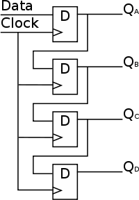
There are two common types of registers:
- Parallel load Register
- Shift Register.
what is the parallel load register?
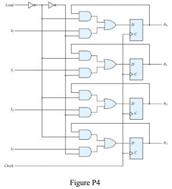
In digital systems, a register with parallel load is a fundamental building element. It is critical that you have a complete knowledge of their actions. A master clock generator provides a constant train of clock pulses in synchronous digital systems. The pulses are sent to all of the system’s flip-flops and registers. The master clock functions like a drum, providing a steady beat to all elements of the system. At each clock pulse, a different control signal must be utilized to determine which register operation will be executed.
Loading or updating a register refers to the process of transferring new data into it. We say that the downloading is done in parallel if all the bits of the register are loaded at the same time using a common clock pulse. When a clock edge is applied to the register’s C input, all four inputs are loaded in parallel. If the data of the register must be kept constant, the input must be remained constant or the clock must be disabled in this arrangement. The data bus that drives the register in the first scenario would be unavailable for other operations. In the second scenario, the clock can be prevented from reaching the register by using an activating gate to regulate the clock input signal.
Trying to insert gates into the clock route, on the other hand, is a bad idea since it implies that logic is essential with clock pulses. The addition of logic gates causes a difference in propagation delays between the master clock and the flip-flop inputs. To properly synchronize the system, all clock pulses must arrive at the same moment across the system.
As a result, all of the flip-flops will activate at the same time. Using clock pulses to perform logic introduces unpredictable delays and may cause the system to lose synchronization. As a result, rather of regulating the clock via the flip-flops’ C inputs, it is preferable to control the register’s operation using the D inputs. This produces the effect of a gated clock without affecting the circuit’s clock route.
A four-bit data storage register having a load control input connected to the D inputs of the flip flops via gates. The extra gates construct a two-channel mux, with the output driving the register’s input with either the data bus or the register’s output. The action to be done with each clock pulse is determined by the load input to the register. The data from the four external inputs is transmitted into the register on the next positive edge of the clock when the load input is 1.
The outputs of the flip-flops are linked to their corresponding inputs when the load input is 0. Because a D flip-flop does not have a no-change condition, the feedback link from output to input is required. The D input determines the next state of the register with each clock edge. Make the D input equal to the current value of the output if you want the output to stay the same.
The clock pulses are continuously applied to the C inputs. The load input controls whether the following pulse accepts new data or keeps the existing data in the register. The transfer of data from the information inputs or the outputs of the register is done at the same time with all four bits in response to a clock edge.
Also read here
what are the serial transfer and serial shift properties of shift registers?