Table of Contents
=Introduction
The common emitter amplifier is a widely used transistor amplifier configuration that plays a crucial role in various electronic circuits. It provides amplification of signals with high voltage gain, making it suitable for applications requiring signal amplification.
Transistors, specifically bipolar junction transistors (BJTs), are the fundamental building blocks of the common emitter amplifier. The common emitter configuration is chosen due to its favorable characteristics, including reasonable input impedance, good voltage gain, and the ability to drive moderately low output impedance.
The main purpose of the common emitter amplifier is to take a weak input signal and amplify it to a higher voltage or power level. This amplified signal can then be used for further processing, transmission, or driving other components in a circuit.
The common emitter amplifier finds widespread use in various fields. It is commonly utilized in audio amplifiers to amplify low-level audio signals, ensuring sufficient power for speakers. Additionally, it is employed in radio frequency (RF) amplifiers to boost weak RF signals received from antennas. The common emitter configuration’s versatility and ability to provide high gain make it a valuable component in many electronic systems.
Transistor Basics:
Transistors are semiconductor devices that play a vital role in modern electronic circuits. They are widely used for amplification, switching, and signal processing purposes. The common emitter amplifier relies on the operation of bipolar junction transistors (BJTs).
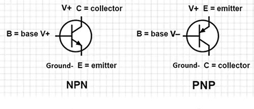
BJTs come in two main types: NPN (negative-positive-negative) and PNP (positive-negative-positive). The NPN transistor is the most commonly used in common emitter amplifier configurations. It consists of three layers of semiconductor material: the emitter, base, and collector.
The emitter is heavily doped with impurities to increase its conductivity, while the base is lightly doped. The collector is moderately doped and larger in size compared to the other two layers. The interface between the emitter and base forms a P-N junction, while the interface between the base and collector forms another P-N junction.
Transistors operate based on the principle of minority carrier injection and control. When a voltage is applied across the base-emitter junction, it forward biases the junction. This allows minority carriers (holes in the NPN transistor and electrons in the PNP transistor) to flow across the junction.
In the common emitter configuration, the base terminal is the input, and the emitter and collector are the output terminals. The transistor acts as a current amplifier, where a small input current flowing into the base controls a larger output current flowing through the collector.
The transistor’s amplification ability is governed by its current gain, known as the beta (β) or hFE value. This value represents the ratio of the collector current (IC) to the base current (IB). Typically, NPN transistors have a β value in the range of 50 to 100, meaning the collector current can be 50 to 100 times larger than the base current.
The transistor’s operation is highly dependent on its biasing conditions. Biasing refers to the application of DC voltages and currents to establish the transistor’s operating point. In the common emitter amplifier, the biasing arrangement ensures the transistor operates in its active region, allowing the amplified signal to be faithfully reproduced.
Common Emitter Amplifier Configuration:
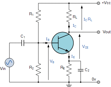
- Transistor Configuration: The common emitter amplifier utilizes a bipolar junction transistor (BJT), specifically an NPN transistor for this explanation. The NPN transistor consists of three layers of semiconductor material: the emitter, base, and collector. The emitter is heavily doped, the base is lightly doped, and the collector is moderately doped.
- DC Biasing: To ensure the transistor operates in its active region, a DC biasing arrangement is employed. The biasing arrangement establishes a stable operating point for the transistor. It typically includes resistors and a power supply.
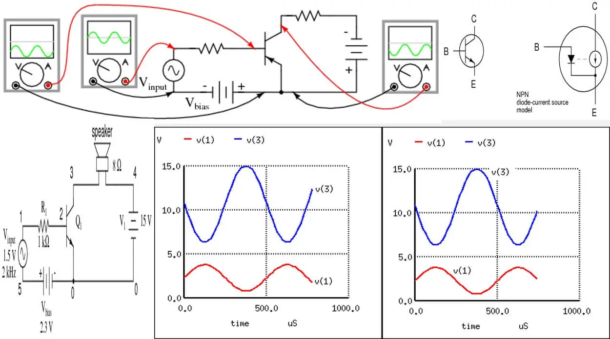
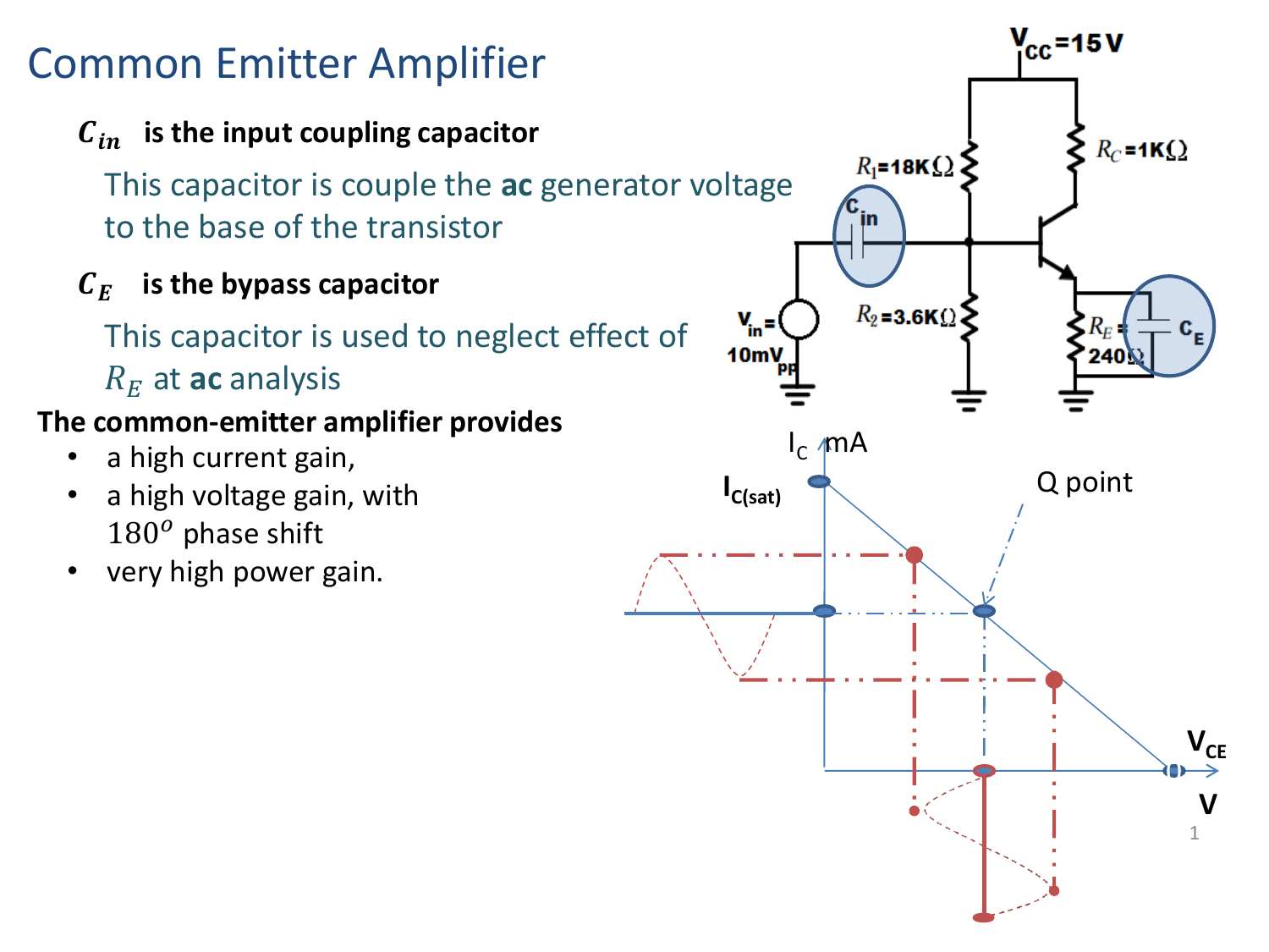
- Signal Input: The input signal is applied to the base terminal through a coupling capacitor (C1). The coupling capacitor blocks the DC component of the input signal, allowing only the AC component to pass. This prevents any interference from the DC biasing arrangement.
- AC Amplification: When an AC signal is applied to the base terminal, it modulates the base current, resulting in an amplified AC signal at the collector. The amplified signal appears across the collector resistor (RC), which is connected between the collector terminal and the supply voltage.
- Output Coupling: An output coupling capacitor (C2) is used to remove the DC component from the amplified signal and extract only the AC component. This allows the amplified AC signal to be further processed or sent to subsequent stages in the circuit.
- Voltage Gain: The common emitter amplifier provides voltage amplification. The voltage gains (Av) is determined by the ratio of the output voltage (Vout) to the input voltage (Vin). The typical voltage gain formula for a common emitter amplifier is Av = -RC / RE. The negative sign indicates that the output signal is inverted compared to the input signal.
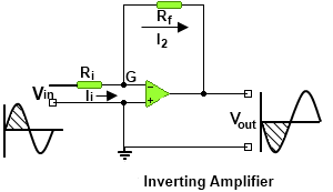
- Inverting Configuration: The common emitter amplifier is an inverting amplifier. This means that a positive voltage changes at the base terminal results in a negative voltage change at the collector terminal. The output signal is phase-reversed compared to the input signal.
- Frequency Response: The frequency response of the common emitter amplifier depends on the external components and the intrinsic characteristics of the transistor. The upper cutoff frequency (fT) is the frequency at which the gain starts to decrease. It is determined by the transistor’s transition frequency and the values of the external components.
- Biasing Stability: The stability of the common emitter amplifier is essential for proper operation. Variations in temperature, transistor characteristics, and component tolerances can affect the bias point. Techniques like negative feedback and thermal compensation may be employed to enhance stability.
Common Emitter Amplifier Configuration:
DC biasing is a crucial aspect of the common emitter amplifier configuration. It involves setting up the proper DC voltages and currents to establish a stable operating point for the transistor. The DC biasing arrangement ensures that the transistor operates within its active region, allowing for accurate amplification of the input signal.
The key components involved in DC biasing are the emitter resistor (RE), base resistor (RB), and the biasing network.
- Emitter Resistor (RE):
- The emitter resistor (RE) is connected between the emitter terminal and the ground (common reference point).
- RE provides negative feedback, stabilizes the operating point, and improves the stability and linearity of the amplifier.
- It sets the emitter current (IE) and helps establish the voltage across the emitter-base junction (VBE).
- Base Resistor (RB):
- The base resistor (RB) is connected between the base terminal and the biasing network.
- RB limits the base current (IB) flowing into the transistor and helps control the operating point.
- It plays a crucial role in preventing excessive base current and maintaining the desired bias conditions.
- Biasing Network:
- The biasing network, typically a voltage divider, establishes the appropriate voltage at the base terminal.
- It consists of resistors connected between the power supply voltage (VCC) and the ground.
- The resistors divide the supply voltage to provide the desired bias voltage (VBB) at the base.
- The bias voltage determines the base-emitter voltage (VBE) and helps establish the operating point.
AC Signal Amplification in The Common Emitter Amplifier Configuration:
AC signal amplification is a key function of the common emitter amplifier. It involves the amplification of the AC component of the input signal, while the DC component is blocked or bypassed.
- Input Signal Coupling:
- The AC input signal is applied to the base terminal of the transistor through a coupling capacitor (C1).
- The coupling capacitor blocks the DC component of the input signal, allowing only the AC component to pass through.
- This prevents any interference from the DC biasing arrangement and ensures that only the desired AC signal reaches the base terminal.
- Base Current Modulation:
- When the AC signal is applied to the base terminal, it modulates the base current (IB) flowing into the transistor.
- The variations in the base current cause corresponding variations in the collector current (IC).
- Current Gain:
- The transistor’s current gain, represented by the beta (β) or hFE value, determines the amplification factor of the AC signal.
- The beta value represents the ratio of the collector current (IC) to the base current (IB). Typically, NPN transistors have a beta value in the range of 50 to 100.
- This means that a small change in the base current results in a significantly larger change in the collector current.
Voltage Gain:
- The amplified AC signal appears across the collector resistor (RC), which is connected between the collector terminal and the supply voltage.
- The voltage gain (Av) of the common emitter amplifier is determined by the ratio of the output voltage (Vout) to the input voltage (Vin).
- The typical voltage gain formula for a common emitter amplifier is Av = -RC / RE, where RC is the collector resistor and RE is the emitter resistor.
- The negative sign indicates that the output signal is phase-reversed compared to the input signal, making the common emitter amplifier an inverting amplifier.
Output Coupling:
-
- After the AC signal is amplified, an output coupling capacitor (C2) is used to remove the DC component from the amplified signal.
- The coupling capacitor blocks the DC voltage and allows only the amplified AC signal to pass through.
- This prepares the signal for further processing or transmission to subsequent stages in the circuit.
Voltage Gain in The Common Emitter Amplifier:
Voltage gain is a crucial parameter in the common emitter amplifier configuration. It represents the amplification factor of the input voltage signal and indicates how much the output voltage is magnified relative to the input voltage.
-
Formula for Voltage Gain:
- The typical formula for voltage gain (Av) in a common emitter amplifier is Av = -RC / RE, where RC is the collector resistor and RE is the emitter resistor.
- The negative sign indicates that the output signal is phase-reversed compared to the input signal, making the common emitter amplifier an inverting amplifier.
- The magnitude of the voltage gain is determined by the ratio of these resistors.
-
Impact of Collector Resistor (RC):
- The collector resistor (RC) plays a crucial role in determining the voltage gain.
- Increasing the value of RC leads to a higher voltage gain, as it allows more voltage to be developed across it for a given output current.
- However, increasing RC also reduces the available voltage swing and can limit the output voltage swing range
-
Impact of Emitter Resistor (RE):
- The emitter resistor (RE) also affects the voltage gain.
- A larger value of RE reduces the voltage gain, as it reduces the voltage developed across the emitter terminal.
- However, increasing RE enhances stability and linearity by providing negative feedback and improving bias stability.
-
Influence of Biasing Conditions:
- The biasing conditions of the transistor, established through the DC biasing arrangement, have a direct impact on voltage gain.
- Proper biasing ensures that the transistor operates in its active region and provides the desired amplification.
- Biasing conditions affect the operating point and determine the quiescent current and voltage levels of the amplifier.
Load Line Analysis:
- Load line analysis is a graphical technique used to understand the voltage gain characteristics of the common emitter amplifier.
- By plotting the collector current (IC) versus collector-emitter voltage (VCE) on a load line graph, the voltage gain can be determined at different operating points.
- The slope of the load line represents the output impedance, and the intersection of the load line and the transistor’s characteristic curve determines the operating point and voltage gain.
Optimizing Voltage Gain:
- The selection of appropriate values for RC and RE allows for the optimization of voltage gain.
- The choice of these resistors depends on specific requirements such as desired gain, stability, linearity, and available supply voltage.
- Designers must also consider trade-offs between gain, stability, bandwidth, and other performance parameters.
Input and Output Impedance in The Common Emitter Amplifier:
Input Impedance:
- The input impedance of the common emitter amplifier refers to the impedance seen by the input signal source connected to the base terminal.
- The input impedance is relatively moderate in the common emitter configuration, typically in the range of a few kilo ohms to tens of kilo ohms.
- The input impedance is influenced by the base-emitter junction impedance and the base current.
- Base-Emitter Junction Impedance: The input impedance is primarily determined by the forward-biased base-emitter junction of the transistor. The impedance is inversely proportional to the transconductance (gm) of the transistor.
- Base Current: The input impedance also depends on the base current flowing into the transistor. The higher the base current, the lower the input impedance.
- Coupling Capacitor: The coupling capacitor (C1) used to block the DC component of the input signal does not significantly affect the input impedance at signal frequencies, as it has a high impedance for AC signals.
Output Impedance:
-
- The output impedance of the common emitter amplifier refers to the impedance seen by the load connected to the collector terminal.
- The output impedance of the common emitter amplifier is typically low, typically in the range of a few hundred ohms to a few kilo ohms.
- The low output impedance is mainly attributed to the presence of the collector resistor (RC) in parallel with the output signal path.
- Collector Resistor (RC): The presence of the collector resistor helps in reducing the output impedance by providing a low-resistance path for the output signal.
- Miller Effect: The output impedance is also influenced by the Miller effect, which arises due to the capacitance between the collector and base terminals. The effect reduces the effective impedance at higher frequencies.
Importance of Input and Output Impedance:
-
-
- The input impedance is important as it determines the loading effect on the signal source connected to the base terminal. A higher input impedance minimizes the signal source’s loading and allows for effective signal transfer.
- The low output impedance is crucial for delivering the amplified signal to the load without significant loss or distortion. It ensures efficient power transfer and minimizes the impact of load impedance variations.
-
Impedance Matching:
-
-
-
- Impedance matching is an important consideration in amplifier design. It involves matching the impedance of the amplifier with the impedance of the preceding and following stages to ensure efficient signal transfer.
- Impedance matching can be achieved through appropriate selection of coupling capacitors, biasing resistors, and load resistors. Transformers and matching networks can also be used for impedance matching purposes.
-
-
Inverting Amplification in The Common Emitter Amplifier:
Inverting Amplification:
-
- The common emitter amplifier is an inverting amplifier, meaning that the output signal is phase-reversed compared to the input signal.
- When a positive voltage change is applied to the input signal, the output voltage of the amplifier undergoes a corresponding negative voltage change.
Transistor Operation:
-
- In the common emitter configuration, the input signal is applied to the base terminal of the transistor.
- The transistor’s behavior is determined by the relationship between the base-emitter voltage (VBE) and the collector-emitter voltage (VCE).
- When the base-emitter junction is forward-biased, a small change in the base-emitter voltage results in a larger change in the collector current (IC).
- The amplified AC signal appears across the collector resistor (RC), causing a corresponding voltage change at the output.
Signal Polarity Reversal:
-
- The inverting nature of the common emitter amplifier can be understood by considering the current flow in the collector circuit.
- An increase in the base current (IB) causes an increase in the collector current (IC).
- As a result, the voltage drop across the collector resistor (RC) increases, leading to a decrease in the output voltage.
- Conversely, a decrease in the base current results in a decrease in the collector current and an increase in the output voltage.
Phase Reversal:
-
- The phase reversal occurs due to the transistor’s intrinsic properties and the common emitter configuration.
- As the input signal causes changes in the base current, these changes are reflected in the amplified output signal.
- However, due to the transistor’s behavior, a positive change at the input leads to a negative change in the output, resulting in phase reversal.
- Applications of Inverting Amplification:
- The inverting nature of the common emitter amplifier can be advantageous in many applications.
- It is particularly useful in audio applications where phase inversion is desired, such as in certain audio processing and feedback systems.
- In communication systems, inverting amplifiers are commonly used in mixers and modulators.
- Compensation Techniques:
- In certain applications where maintaining the original signal polarity is crucial, compensation techniques can be employed.
- Feedback mechanisms, such as using an additional inverting stage or employing phase-shifting networks, can be used to restore the original signal polarity while retaining the amplification benefits of the common emitter configuration.
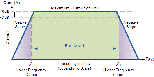
Frequency Response in The Common Emitter Amplifier:
Frequency Response:
-
- The frequency response of the common emitter amplifier refers to how the amplifier’s gain varies with different frequencies of the input signal.
- It is important to analyze the frequency response to ensure the amplifier performs optimally across the desired frequency range.
External Components:
-
-
- The frequency response of the common emitter amplifier is influenced by the external components in the circuit, such as resistors and capacitors.
- The values of these components affect the amplifier’s gain and bandwidth.
-
Capacitors:
-
- Coupling Capacitor (C1): The coupling capacitor (C1) blocks the DC component of the input signal, allowing only the AC component to pass through to the base terminal.
- Bypass Capacitor (C3): The bypass capacitor (C3) is used to bypass the emitter resistor (RE). It improves the amplifier’s low-frequency response by shorting the emitter resistor for AC signals.
Intrinsic Capacitances:
-
-
- The transistor itself possesses intrinsic capacitances that impact the frequency response of the common emitter amplifier.
- Base-Collector Capacitance (CBC): The base-collector capacitance (CBC) appears as a parasitic capacitance between the base and collector terminals of the transistor. It affects the high-frequency response of the amplifier.
- Base-Emitter Capacitance (CBE): The base-emitter capacitance (CBE) is the capacitance between the base and emitter terminals of the transistor. It can cause Miller effect and affect the high-frequency response.
-
Bandwidth:
-
-
-
- The bandwidth of the common emitter amplifier represents the frequency range over which the amplifier’s gain remains relatively constant.
- The upper cutoff frequency (fT) is an important parameter that determines the bandwidth.
- The upper cutoff frequency is influenced by the intrinsic capacitances of the transistor and the values of external components.
- It is typically determined by the transistor’s transition frequency (fT) and the values of coupling capacitors, resistors, and the collector load.
-
-
Frequency Compensation Techniques:
-
-
-
-
- To extend the frequency response and increase the bandwidth, various frequency compensation techniques can be employed.
- Techniques like neutralization, cascade configurations, and Miller compensation can be used to minimize the impact of parasitic capacitances and improve the amplifier’s high-frequency response.
-
-
-
Trade-Offs:
-
- Designing the frequency response of the common emitter amplifier involves trade-offs between gain, bandwidth, stability, and other performance parameters.
- Increasing the gain can result in a narrower bandwidth, while widening the bandwidth may lead to reduced gain.
- Designers need to carefully select component values and optimize the circuit to achieve the desired trade-offs based on specific requirements.
Biasing Stability in The Common Emitter Amplifier:
Importance of Biasing Stability:
-
- Biasing stability is crucial in the common emitter amplifier to ensure the transistor operates in its active region and maintains a stable operating point.
- The stable biasing of the amplifier is necessary to prevent distortion, maintain linearity, and achieve consistent amplification of the input signal.
Factors Affecting Biasing Stability:
-
-
- Temperature Variations: Temperature changes can significantly affect the characteristics of the transistor, including the base-emitter voltage (VBE) and the current gain (β). This can cause variations in the operating point and lead to distortion or even transistor failure.
- Transistor Characteristics: Variations in transistor parameters, such as the β value and VBE, due to manufacturing tolerances and aging, can impact biasing stability.
- Component Tolerances: Variations in the values of resistors used in the biasing network and other components can affect the operating point.
-
Thermal Compensation:
-
-
-
- Thermal compensation techniques are employed to minimize the effects of temperature variations on biasing stability.
- Temperature-compensating devices, such as diodes or temperature-sensitive resistors (thermistors), can be used in the biasing network to compensate for temperature changes.
- These devices help stabilize the bias voltage and compensate for shifts in VBE caused by temperature variations.
-
-
Negative Feedback:
-
-
-
-
- Negative feedback is commonly used in amplifier circuits to enhance biasing stability.
- It involves feeding back a portion of the output signal to the input in such a way that it opposes any changes in the input signal.
- Negative feedback helps reduce variations in the amplifier’s gain and helps maintain a more stable operating point.
-
-
-
Design Considerations:
- Careful selection of component values is important for biasing stability. It involves considering factors such as temperature ranges, transistor characteristics, and component tolerances.
- Ensuring appropriate voltage levels at the base terminal, proper biasing current, and suitable resistor values in the biasing network are crucial for maintaining stability.
- Use of stable and reliable components, as well as proper heat dissipation measures, can also contribute to biasing stability.
Simulation and Testing:
- Simulating the common emitter amplifier circuit and conducting thorough testing can help evaluate biasing stability.
- Performing temperature and tolerance analysis, as well as analyzing the amplifier’s behavior under different conditions, aids in identifying and addressing potential biasing stability issues.
Applications of The Common Emitter Amplifier:
- Audio Amplification:
- One of the most common applications of the common emitter amplifier is in audio amplification.
- It is used in audio systems to amplify low-level audio signals from sources such as microphones, musical instruments, or audio players.
- Common emitter amplifiers provide high voltage gain and can drive speakers or headphones to produce audible sound.
- RF Amplification:
- The common emitter amplifier is widely used in radio frequency (RF) amplification circuits.
- It is utilized to amplify weak RF signals received from antennas in communication systems, wireless devices, and radio receivers.
- RF amplifiers based on the common emitter configuration enhance the signal strength before further processing or transmission.
- Instrumentation Amplification:
- The common emitter amplifier is employed in instrumentation applications where precise signal amplification and measurement are required.
- It is used in instrumentation amplifiers for signal conditioning, data acquisition systems, and measurement equipment.
- Signal Processing:
- The inverting nature of the common emitter amplifier makes it suitable for certain signal processing applications.
- Inverting amplifiers are used in analog signal processing circuits, such as filters, oscillators, and mixers, where phase inversion is required.
- Feedback Systems:
- The common emitter amplifier is a key component in feedback systems.
- It is used in feedback configurations to stabilize amplifiers, control gain, and improve linearity and stability.
- Negative feedback can be employed to enhance biasing stability and reduce distortion.
Analog-to-Digital Conversion:
- In some analog-to-digital conversion systems, common emitter amplifiers are utilized as preamplifiers.
- They amplify weak analog signals from sensors or transducers before conversion into digital form by analog-to-digital converters (ADCs).
Oscillators:
- The common emitter amplifier can be incorporated into oscillator circuits to generate periodic waveforms.
- It is used in oscillator designs, such as the Colpitts or Hartley oscillators, where the amplification provided by the common emitter configuration is critical for sustaining oscillation.
Voltage Level Shifting:
- Common emitter amplifiers can be used for voltage level shifting applications.
- They can shift the voltage level of an input signal to a different range, making it compatible with other circuitry or devices.
Automotive Electronics:
- The common emitter amplifier finds application in automotive electronics.
- It is used in audio systems, engine control units, sensors, and various other electronic components in vehicles.
Performance Enhancement Techniques for The Common Emitter Amplifier:
- Negative Feedback:
- Negative feedback is a widely used technique to enhance the performance of the common emitter amplifier.
- It involves feeding a portion of the output signal back to the input in such a way that it opposes any changes in the input signal.
- Negative feedback helps improve linearity, reduce distortion, increase stability, and extend the bandwidth of the amplifier.
- It can be achieved through various feedback configurations, such as voltage feedback or current feedback.
- Frequency Compensation:
- Frequency compensation techniques are employed to address stability and frequency response issues in the common emitter amplifier.
- Techniques like neutralization, Miller compensation, and pole-zero compensation are used to minimize the impact of parasitic capacitances and improve high-frequency response.
- These techniques help maintain stability, reduce phase shift, and enhance the amplifier’s overall frequency response.
- Thermal Stabilization:
- Temperature variations can significantly affect the performance of the common emitter amplifier.
- Thermal stabilization techniques, such as thermal feedback and thermal compensation, are employed to mitigate the impact of temperature changes.
- These techniques involve using temperature-sensitive components, such as diodes or thermistors, in the biasing network to compensate for temperature variations and stabilize the operating point.
- Cascade Configuration:
- The cascade configuration is a performance enhancement technique that combines multiple transistors to improve various amplifier parameters.
- In the cascade configuration, two transistors are connected in series, with one acting as a common emitter amplifier and the other as a common base amplifier.
- The cascade configuration helps increase gain, bandwidth, and input/output impedance while reducing distortion and improving linearity.
- Darlington Pair:
- The Darlington pair is another technique used to enhance the performance of the common emitter amplifier.
- It involves connecting two transistors in a configuration where the output of the first transistor is connected to the base of the second transistor.
- The Darlington pair provides high current gain and can be used to drive loads with high current requirements while maintaining good linearity.
- Bootstrapping:
- Bootstrapping is a technique used to enhance the input impedance of the common emitter amplifier.
- It involves connecting a capacitor between the base terminal and the collector terminal, creating a voltage boost.
- The bootstrapping technique effectively increases the input impedance, allowing for better signal transfer and reducing the loading effect on the signal source.
- Active Load:
- Using an active load, such as a current mirror or a constant current source, instead of a simple resistor, can improve the performance of the common emitter amplifier.
- Active loads provide higher output impedance, improved linearity, and increased gain, resulting in better overall amplifier performance.
Trade-Offs Involved in The Design of the Common Emitter Amplifier:
- Gain versus Bandwidth:
- There is a trade-off between the gain and bandwidth of the common emitter amplifier.
- Increasing the gain often results in a narrower bandwidth, while widening the bandwidth may lead to reduced gain.
- Designers need to carefully select component values and optimize the circuit to achieve the desired trade-off between gain and bandwidth based on specific application requirements.
- Stability versus Gain:
- Increasing the gain of the common emitter amplifier can lead to reduced stability.
- Higher gain amplifiers are more susceptible to oscillations and can be prone to instability.
- Techniques such as frequency compensation, feedback, and stability analysis are employed to maintain stability while achieving the desired gain.

3. Linearity versus Distortion:
-
- Linearity and distortion are important trade-offs in amplifier design.
- Increasing the gain of the common emitter amplifier can lead to nonlinear behavior and distortion in the output signal.
- Techniques such as negative feedback, careful biasing, and proper component selection are employed to improve linearity and minimize distortion.
4. Power Dissipation versus Efficiency:
-
- The common emitter amplifier can consume significant power, especially when driving loads with low impedance.
- Higher gain configurations tend to dissipate more power due to increased current flow.
- Designers need to strike a balance between power dissipation and efficiency to ensure optimal performance and avoid overheating.
5. Input Impedance versus Noise:
-
- The input impedance of the common emitter amplifier affects the loading on the input signal source.
- Higher input impedance minimizes the loading effect but can also increase the susceptibility to noise and interference.
- Designers need to optimize the input impedance to strike a balance between loading effects and noise considerations.
6. Output Impedance versus Load Compatibility:
-
- The output impedance of the common emitter amplifier affects the ability to drive different load impedances.
- Lower output impedance allows for better power transfer and compatibility with various loads.
- However, lower output impedance can also lead to increased power dissipation and reduced voltage swing capability.
7. Complexity versus Cost:
-
- Adding performance enhancement techniques, such as frequency compensation or cascode configurations, can increase the complexity and cost of the common emitter amplifier circuit.
- Designers need to consider the trade-off between added complexity and the desired performance improvements while considering overall cost constraints.
Summary:
The common emitter amplifier is a widely used transistor amplifier configuration that provides high voltage gain and moderate input impedance. It consists of a bipolar junction transistor (BJT) with three terminals: emitter, base, and collector.
- The common emitter amplifier is an inverting amplifier, where the output signal is phase-reversed compared to the input signal.
- DC biasing is crucial for establishing a stable operating point for the transistor. It ensures the transistor operates in its active region and provides accurate amplification.
- The input signal is applied to the base terminal through a coupling capacitor, allowing only the AC component to pass through.
- AC signal amplification is achieved by modulating the base current, resulting in amplified AC signal at the collector. The voltage gain is determined by the ratio of the collector resistor to the emitter resistor.
- The common emitter amplifier provides moderate input impedance and high voltage gain, making it suitable for audio amplification, RF amplification, and other applications.
- The frequency response of the common emitter amplifier depends on external components and the intrinsic characteristics of the transistor. Techniques like frequency compensation and feedback are used to optimize the frequency response.
- Biasing stability is crucial for maintaining the operating point of the transistor. Techniques such as thermal compensation and negative feedback are employed to enhance biasing stability.
- Performance enhancement techniques, such as negative feedback, frequency compensation, and thermal stabilization, can be employed to improve the amplifier’s performance.
- Designing the common emitter amplifier involves trade-offs between parameters such as gain, bandwidth, stability, linearity, power dissipation, and cost.
- Understanding the common emitter amplifier configuration and its characteristics enables engineers to design circuits that accurately amplify signals according to specific requirements.
DC Analysis of Common Emitter Amplifier
AC Analysis of Common Emitter Amplifier