The PN junction diode
What is the barrier potential of PN junction diode? The barrier potential is the amount of the energy that is required by any charge to overcome for crossing one junction. If a charge has this much energy then it will be able to move across the regions (P and N). A p-type material comprises of silicon and trivalent materials, for example, boron. The boron adds an extra hole when it bonds with the silicon molecules. Since the number of protons and electrons are equivalent throughout the material, there is no net charge in the material thus it is neutral.
A n-type silicon material comprises of silicon atoms and pentavalent materials, for example, antimony. As you have seen, an impurity atom releases an electron when it bonds with four silicon atoms. Since there is as yet an equivalent number of protons and electrons (counting the free electrons) throughout the material, there is no net charge in the material thus it is neutral. If one part of a Silicon material is doped such that one side is p-type and other side is n-type, then a PN-Junction is obtained at the boundary between p and n region and the resulting device is called diode.
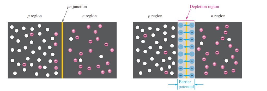
The p-region has holes as majority charge carriers while very few thermally generated minority charge carriers (electrons). These majority charge carriers are because of the added impurities. The n-region has electrons as majority charge carriers because of impurities and very few thermally generated holes. It can be seen clearly in the following figure.
Formation of the Depletion Region
The free electrons in the n-region move freely in all directions. The electrons in the n region, diffuse in p-region and combines with holes of p-region. Once they start combining with the holes near the pn-junction, n-region starts losing its electrons and there comes a time when no more diffusion is possible because of the development of depletion region.
Since the n-region is depleted of its electrons, it is shown as a layer of positive charges along the junction. Similarly the p-region, loses its holes during recombination process so a layer of negative charges is developed across the junction. This layer which is composed of because of depletion of charges in both regions is called depletion region as shown in above figure.
Why the name “depletion region” is given?
The name depletion region is given since both regions are depleted of their charges. The formation of depletion region happens so fast. Thus width of depletion region is very low as compared to p and n region.
After the initial diffusion of electrons, there is an equilibrium set that stops further diffusion of electrons across the pn-junction. Basically with the initial diffusion of electrons, a layer of negative charges is developed in p-region that actually distracts the further coming electrons. Hence no more electrons diffusion is possible. Hence depletion region acts as barrier for further movement of electrons across the pn-junction.
What is the barrier potential?
Whenever there is a positive and a negative charge, there is a certain amount of energy that acts on them that can be determined from Coulomb’s Law. This force acts as a force field. Since there is a layer of positive and negative charges across the junction, so there is a force field present in depletion region. Any charge trying to move across the regions needs energy more than this barrier potential. The potential difference of electric field across the depletion region is the amount of voltage required to move electrons through the electric field. This potential is named as barrier potential.
Energy Diagrams of the PN Junction and Depletion Region
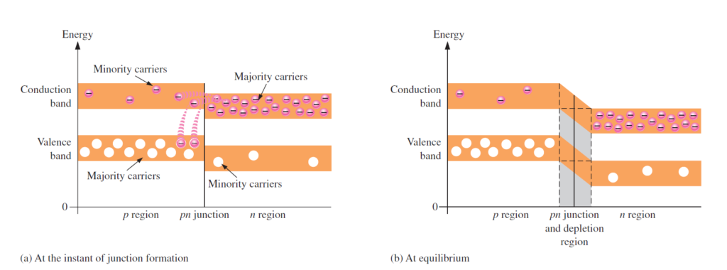
The valence and conduction groups in a n-type material are at somewhat lower energy levels than the valence and conduction groups in a p-type material. Review that p-type material has trivalent debasements and n-type material has pentavalent contaminations. The trivalent contaminations apply lower powers on the external shell electrons than the pentavalent debasements. The lower powers in p-type materials imply that the electron circles are marginally bigger and subsequently have more prominent energy than the electron circles in the n-type materials.
An energy chart for a pn intersection at the moment of arrangement is appeared in Figure below. As should be obvious, the valence and conduction groups in the n district are at lower energy levels than those in the p district, however there is a lot of covering. The free electrons in the n district that possess the upper piece of the conduction band in terms of their energy can undoubtedly diffuse across the intersection (they don’t need to acquire extra energy) and briefly become free electrons in the lower part of the p-locale conduction band. In the wake of intersection the intersection, the electrons rapidly lose energy and fall into the openings in the p-district valence band as demonstrated in Figure below(a). As the dissemination proceeds, the consumption district starts to shape and the energy level of the n-locale conduction band diminishes. The decline in the energy level of the conduction band in the n locale is because of the deficiency of the higher-energy electrons that have diffused across the intersection to the p area. Before long, there are no electrons left in the n-district conduction band with enough energy to get across the intersection to the p-area conduction band, as demonstrated by the arrangement of the highest point of the n-district conduction band and the lower part of the p-area conduction band in Figure (b). Now, the intersection is at balance; also, the exhaustion area is finished in light of the fact that dissemination has stopped. There is an below energy gradient across the consumption area which goes about as an “energy slope” that a n-locale electron should move to get to the p district. Notice that as the energy level of the n-district conduction band has moved descending, the energy level of the valence band has likewise moved descending. It actually takes the equivalent measure of energy for a valence electron to turn into a free electron. At the end of the day, the energy hole between the valence band and the conduction band stays as before.
Also read here:
https://eevibes.com/what-is-the-drift-and-diffusion-current-of-a-diode/