What is the Flag Register of PIC Microcontroller?
What is the Flag Register of PIC Microcontroller? In general, PIC flag register is an 8-bit register. It is also referred to as status register. Even though status register is 8-bits wide, only 5 of its bits are used by the PIC18. The three unused bits are not used and are read as 0. The 5 flags are called conditional flags, meaning that they tell us about some conditions that are resulted when the instructions are executed. These 5 flags are C (carry), DC (digital carry), Z (zero), OV (over flow) and N (negative).
See the figure below for the bits of the status register. Each of the conditional flags can be used to perform a conditional branch jump.

1. C – (carry flag)
2. DC – (digital carry flag)
3. Z – (zero flag)
4. OV – (Over flow flag)
5. N – (Negative flag)
6. X – D5, D6 and D7 are not used, and reserved for future use.
What are the flag registers of PIC? The following is the explanation of the flag bits in PIC status register, and the impact of different instructions on this register will be discussed after.
C (the carry flag)
The carry flag is set whenever there is a carry out from the D7 bit. This flag bit gets affected after an 8-bit addition or subtraction.
DC (the digital carry flag)
The digital carry flag works, if there is a carry from D3 toD4 during an addition or subtraction operation, then this bit is set, otherwise it is cleared. This flag bit is used by instructions that perform BCD (binary coded decimal) arithmetic. In some other microprocessor’s it is also called AC flag (auxiliary carry flag).
Z (the zero flag)
This flag reflects the result of an arithmetic or logic operation. If the result is zero, then Z=1. The result is not zero if Z=0.
OV (the overflow flag)
The overflow flag is set when the result of a signed number operation is too large, causing the high order bit to overflow into the sign bit. Generally, the carry flag is used to detect errors in unsigned arithmetic operations while the overflow flag is used to detect errors in signed arithmetic operations. The Ov and n flag bits are used for the signed number arithmetic operations.
N (the negative flag)
The negative flag works when, the binary representation of signed numbers uses D7 as the sign bit. The negative flag reflects the result of an arithmetic operation. If we consider the D7 bit of the result is zero, then N = 0 and the result is positive. If we consider the D7 bit is 1, then N = 1 and the result is negative. The negative and OV flag bits are used for the signed number arithmetic operations.
Add instruction and status register
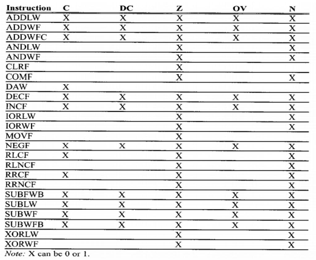
Now we will see the impact of ADDLW instruction on the flag bits c, dc and z of the status register. Although the flag bits C, Z, DC, OV and N are affected by the ADDLW instruction, we will only focus on C, DC, and Z for now. Because they relate only to signed number operations.
Not all instructions affect the flags
Some of the instructions affect all flags C, DC, Z, OV and N. For example, ADDLW. But some instruction affects no flag bits at all. All the move instructions are in this category except MOVF and some instructions affect only the Z or N bit, or both. Those instructions in this category are (e.g., ANDWL).
The table below shows us all the flag bits which are affected by their respective instructions:
Table of instructions that affect flag bits

Flag bits and decision making
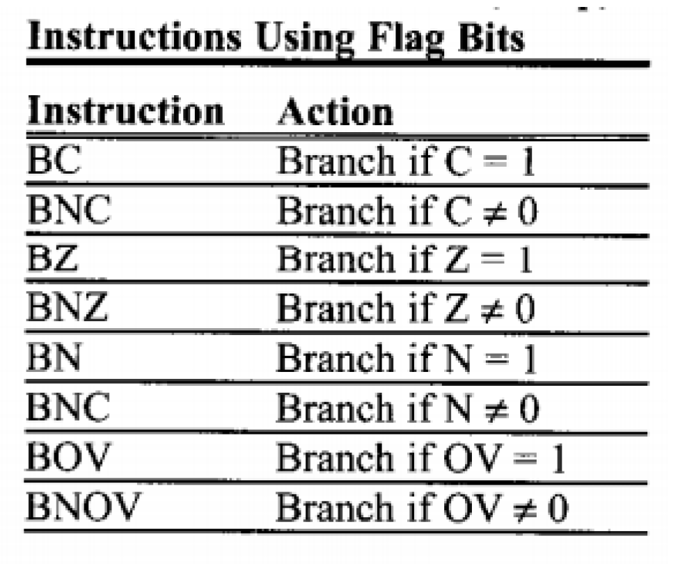
As the status flags are also called conditional flags, there are instructions that will make a conditional jump based on the status of the flag bit.

The examples of two flag registers in PIC series are TXSTA and RCSTA, both of them are explained in detail below:
TXSTA (transmit status and control register)
TXSTA is an 8-bit register used to select the synchronous/asynchronous modes and data framing size, among other things, figure below describes various bits of TXSTA register, the asynchronous mode with a data size of 8-bits. The BRGH bit has been used to select a higher speed for transmission. We will examine the higher transmission rate at the end. Note that the D6 of the TXSTA determines the framing of data by specifying the number of bits per character. We use an 8-bit data size. There are some applications for the 9-th bit in which the ninth bit can be used as an address

The following is the explanation of its bits:
CSRC: Clock Source Select bit (Asynchronous mode: Don’t care, therefore D7 = 0).
TX9: 9-bit Transmit Enable bit
1 = Selects 9-bit transmission 0 = Selects 8-bit transmission (this option is used so, D6 =0)
TXEN: Transmit Enable bit
1 = Transmit enabled 0 = Transmit disabled
We turn on and off this bit in order to start or stop data transfer
SYNC: USART Mode Select bit (D4 =0)
1 = Synchronous mode 0 = Asynchronous mode
BRGH: High Baud Rate Select bit
1 = High speed 0 = Low speed (default)
TRMT: Transmit Shift Register Status bit (TSR status)
1 = TSR empty 0 = TSR full
TX9D: the 9th bit of Transmit Data, can be Parity bit
Can be used as an address or parity bit in some applications.
RCTSA (receive status and control register)
The RCTSA is an 8-bit register used to enable the serial port to receive data, among other things, figure describes various bits of RCTSA register. In this section we use he 8-bit data frame.
SPEN: the Serial Port Enable bit
1 = ,,,Serial port enabled (configures RC7/RX/DT and RC6/TX/CK pins as serial port pins) 0 = Serial port disabled
RX9: the 9-bit Receive Enable bit
1 = Selects 9-bit reception 0 = Selects 8-bit reception
SREN: the Single Receive Enable bit (Asynchronous mode: Don’t care)
CREN: the Continuous Receive Enable bit
Asynchronous mode: 1 = this Enables continuous receive 0 = this Disables continuous receive
ADDEN: The Address Detect Enable bit
Asynchronous mode 9-bit (RX9 = 1): 1 = Enables address detection, enables interrupt and load of the receive buffer when RSR is set 0 = Disable’s address detection, all bytes are received and ninth bit can be used as parity bit
FERR: the Framing Error bit
1 = Framing error (can be updated by reading RCREG register and receive next valid byte) 0 = No framing error
OERR: the Overrun Error bit
1 = gives Overrun error (can be cleared by clearing bit CREN) 0 = No overrun error
RX9D: the 9th bit of Received Data (can be parity bit but must be calculated by user firmware
Also read here
https://eevibes.com/engineering-projects/how-to-control-the-direction-of-dc-motor-with-pic/