Explain how to calculate A/D conversion timings?
Explain how to calculate A/D conversion timings? ADC means analog to digital converter. Basically, it is a data converter that allows digital circuits to communicate with real world and it change analog signal into binary code, when we program it.
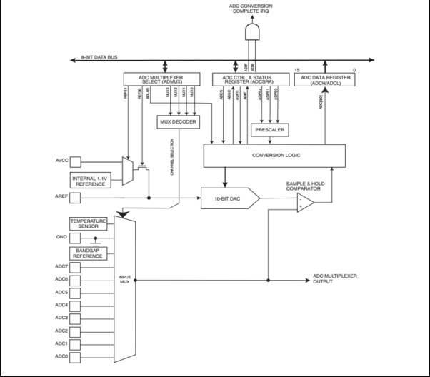
Types of registers linked with ADC programming:
There are different types of registers linked with ADC programming
- ADC Multiplexer select register (ADMUX)
- ADC control and status register A (ADCSRA)
- ADC data register low (ADCL)
- ADC data register high (ADCH)
- ADC control and status register B (ADCSRB)
- DIDR0 that is use to structure hardware and convert analog to digital
ADMUX:
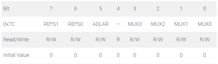
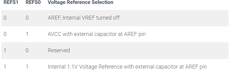
Bit 7:6-REFS[1:0] Reference selection bits
These bits are used to reference the voltage for ADC. If external reference voltage is applied then internal voltage reference options may not use.
Bit 5-ADLAR:
It affects presentation of ADC conversion result is ADC data register. TO left adjust the result should be write one to ADLAR.
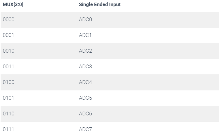
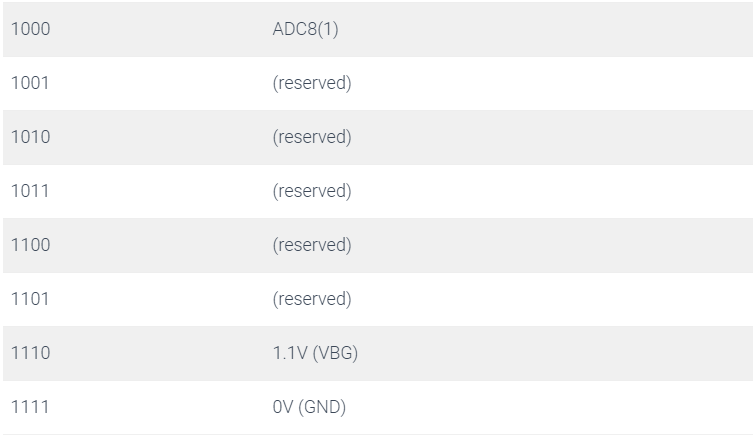
Bits 3:0 – MUX[3:0]: Analog channel selection bits
The value of these bits select that which analog inputs are connected to the ADC.
ADCSRA – ADC control and status register A:
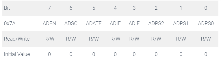
Bit 7-ADEN: ADC Enable
If we write this bit to one then it will enable ADC. But if we write 0 then ADC will turn off. If we turn the ADC off while conversion is in progress, then the conversion will be terminated.
Bit 6 – ADSC: ADC start conversion
In single conversion mode, to start each conversion we have to write this bit one. If it is in free running mode then write this bit to one will take 25 ADC clock cycles instead of normal 13. This first conversion will perform initialization of ADC. It returns 0 when conversion completed.
Bit 5 – ADATE: ADC auto trigger enable
When this bit is written to one auto triggering of ADC will enable. The conversion will started on the +ve edge of selected trigger signal. Trigger source is selected by setting ADC trigger selected bits.
Bit 4 – ADIF: ADC interrupt Flag
When ADC conversion completes and data registers updated then we set this bit. The ADC conversion complete interrupt is executed if the ADIE bit and the I-bit in SREG are set.
Bit 3- ADIE: ADC Interrupt Enable:
ADC conversion complete interrupt will be activated when this bit is written one and I-bit in SREG is set.
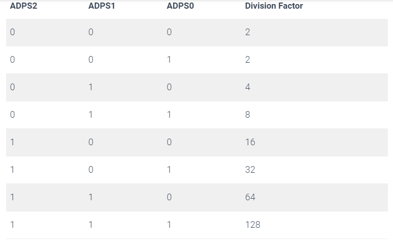
Bits 2:0 – ADPS [2:0]
This type of bit represents the division factor btw system clock frequency and input clock to ADC.
ADCL and ADCH – ADC Data Register
ADLAR=0
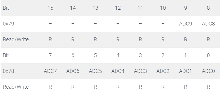
ADLAR=1
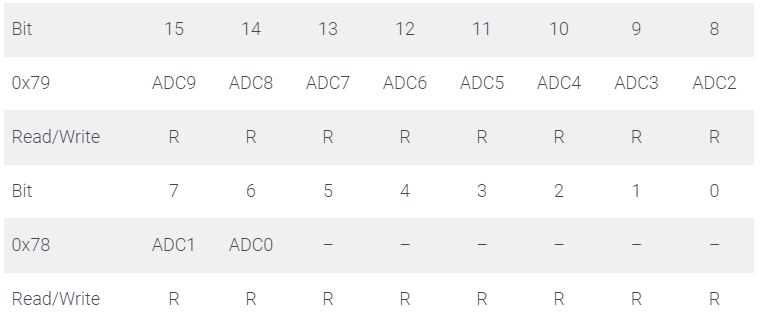
When ADC conversion completed the result is found in these two registers. Total 10bits of conversion result is store in these two registers.
ADCSRB- ADC control and status register BA
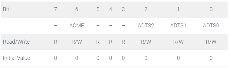
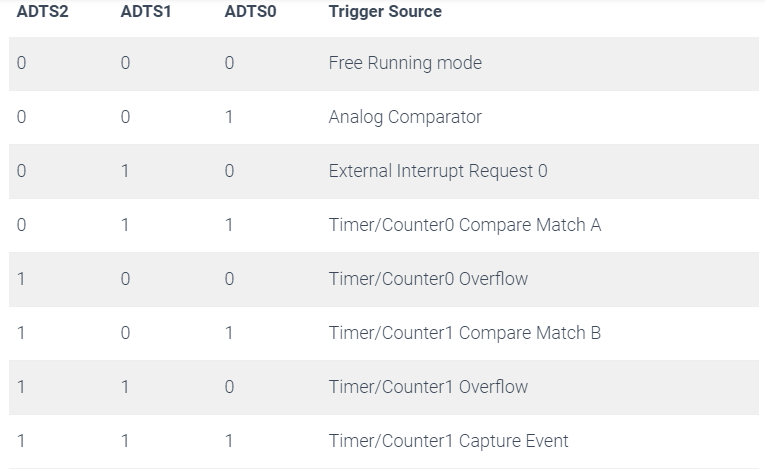
Bit 2:0-ADTS [2:0] ADC auto trigger source
If ADATE in ADCSRA is written to one then value of these types of bits will select that which type of source will trigger an ADC conversions.
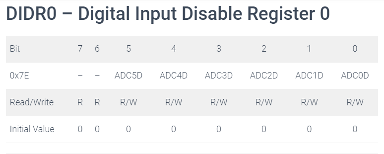
Bit 5:0 ADC5D….ADC0D: ADC5….0 Digital input disable
When this bit is written logic one the digital buffer corresponding pin of ADC will disable The corresponding pin always read as zero when analog signal applied then 0pin and digital input is not needed. Pin will be written logic one because to reduce power consumption in buffer.
Calculate A/D conversion time:
By using ADCS (A/D clock source) bits of both ADCON0 and ADCONI registers we can set A/D conversion time. The conversion time is defined in terms of Tad, Where Tad is conversion time per bit. If we want to calculate Tad then we have to use conversion clock source of Fosc/2, Fosc/4, Fosc/8, Fosc/16, Fosc/32 or Fosc/64, where Fosc is the speed of crystal frequency connected to PIC18 chip. For PIC18, the conversion time will be12 times of tad. Tad cannot be faster than 1.6ms.
We can also use the internal RC oscillator for the conversion in clock source, instead of the Fosc of the external crystal oscillator. In that case the Tad is typically 4-6us and conversion is 12*6us=72us.
There is another timing factor to which we pay attension is the acquisition time (Tacq). After an A/D channel is selected, we must allow some time for the sample and hold capacitor (C hold) to charge fully to the input voltage level present at the channel. It is only after the elapsing of this acquisition time that the A/D conversion can be started. Although many factors (e. g. Vdd and temperature) affect the duration of Tacq, we can use a typical value of 15us. In some newer generations of the PIC 18, we have option of controlling the exact time of tacq by pro-gamming the internal register ADCON2. In the PIC 18F452/458, we have only the ADCON0 and ADCONI registers.
Also read here
https://eevibes.com/computing/discuss-the-characteristics-of-adc-in-detail/