
Standard Printed Circuit Board (PCB) Thickness: A Comprehensive Market Perspective
Printed Circuit Boards (PCBs) serve as the foundational infrastructure for modern electronics, mechanically supporting and electrically connecting components in devices ranging from smartphones to industrial machinery. One critical attribute of PCBs that significantly influences their design, manufacturing, and application is their thickness. Standard PCB thickness, typically measured in millimeters or mils (thousandths of an inch), has evolved over time to meet industry needs, balancing functionality, manufacturability, and cost.
As of March 12, 2025, the global PCB market continues to expand, driven by technological advancements and increasing demand across sectors like consumer electronics, automotive, and telecommunications. This article explores the concept of standard PCB thickness, its historical origins, current market trends, and future implications from a research-based perspective.
Historical Context and Evolution of Standard PCB Thickness
The standard PCB thickness of 1.57 mm (approximately 62 mils) traces its roots to the mid-20th century, during the commercialization of integrated circuits. Early PCBs were constructed using plywood as a prototyping substrate, a material that was readily available and measured about 1/16th of an inch thick—equivalent to 1.57 mm.
As electronics transitioned from discrete components to integrated systems, this thickness became a de facto standard, particularly with the advent of board-to-board connectors and rack-mounted systems.
While not explicitly mandated by industry standards like those from the Institute of Printed Circuits (IPC), this value persisted due to its compatibility with manufacturing processes and component designs of the era.
Today, standard PCB thicknesses have diversified beyond the traditional 1.57 mm to include options like 0.8 mm, 1.0 mm, 2.36 mm, and 3.18 mm, reflecting the growing complexity of electronic applications.

For instance, a four-layer PCB might typically measure 0.8 mm to 1.57 mm, while an eight-layer board could range from 1.57 mm to 3.18 mm, depending on the layer count and design requirements.
This evolution is driven by the need for miniaturization, higher component density, and enhanced performance, as noted in market analyses projecting the PCB industry to grow from USD 84.24 billion in 2025 to USD 106.85 billion by 2030, at a compound annual growth rate (CAGR) of 4.87%.
Factors Influencing PCB Thickness
Several factors determine the ideal thickness of a PCB, including:
Number of Layers – Multilayer PCBs, which can range from 4 to over 40 layers, typically have greater thickness due to the stacking of multiple copper and dielectric layers.
Material Type – Common PCB materials like FR4 (fiberglass-reinforced epoxy), aluminum, and polyimide have varying thicknesses. Aluminum-based PCBs used for LED applications often require different thickness considerations.
Electrical Performance – Signal integrity and impedance control impact the choice of PCB thickness. Thinner PCBs may be used for high-frequency applications to reduce parasitic capacitance and interference.
Mechanical Strength – Applications subjected to mechanical stress, such as automotive and industrial control systems, require thicker boards for durability.
Thermal Management – High-power PCBs need adequate heat dissipation, influencing thickness selection. Heavier copper layers in power circuits increase overall board thickness.
Manufacturing Considerations – Fabrication capabilities and tolerances impact PCB thickness variations. Advanced manufacturing techniques allow for precise control over PCB dimensions.
Market Drivers Influencing PCB Thickness
The PCB market is shaped by several key drivers that influence the adoption and standardization of board thickness. One primary factor is the booming consumer electronics sector, which demands thinner, lighter PCBs to support compact devices like smartphones and wearables.
Research indicates that the standard multilayer PCB segment, often ranging from 0.8 mm to 1.6 mm in thickness, holds a significant market share—approximately 35% as of recent estimates—due to its versatility in supporting complex circuitry in a compact form factor.
The rise of Internet of Things (IoT) devices and 5G technology further amplifies this trend, pushing manufacturers toward thinner boards with high-density interconnects (HDI) to accommodate faster data transmission and smaller footprints.
Conversely, industries such as automotive and aerospace require thicker PCBs to ensure durability and reliability under harsh conditions.
The shift toward electric vehicles (EVs) has spurred demand for robust PCBs—often exceeding 1.57 mm—to support battery management systems and power electronics.
A report forecasts that the automotive PCB segment will experience the highest growth rate through 2035, with rigid PCBs (typically 1.57 mm or thicker) projected to capture nearly 39% of the market share by that time due to their cost-effectiveness and ability to handle higher power loads.
This duality in market needs—thinner boards for consumer gadgets and thicker ones for industrial applications—underscores the importance of standardizing thickness options to optimize production and performance.
Manufacturing Considerations and Cost Implications
From a manufacturing standpoint, standard PCB thicknesses like 1.57 mm remain prevalent because they align with established fabrication processes and equipment capabilities.
Most PCB fabrication houses are optimized to produce boards at this thickness, leveraging readily available materials such as FR-4 (a fiberglass-epoxy laminate) and copper foils of 1 oz (35 µm) or 2 oz (70 µm) thickness. Deviating from these standards—opting for ultra-thin boards (e.g., 0.2 mm) or unusually thick ones (e.g., 6 mm)—can increase production costs due to the need for specialized materials, additional processing steps, or custom stackups.
Example
For example, thinner boards require precise handling to prevent warping, while thicker multilayer boards demand more prepreg layers, driving up material and labor expenses.
Market research highlights that cost optimization is a critical concern for PCB manufacturers, particularly in price-sensitive regions like Asia-Pacific, which accounts for over 56% of global PCB production as of 2023.
Here, companies prioritize standard thicknesses to streamline supply chains and reduce lead times, benefiting from economies of scale.
However, as demand for custom solutions grows—especially in high-end applications like medical devices and satellite systems—manufacturers are expanding their offerings, providing laminate thicknesses ranging from 0.2 mm to over 6 mm to meet bespoke design requirements.
Technological Trends Shaping Thickness Standards
Advancements in PCB technology are redefining thickness standards and their market implications. The adoption of flexible and rigid-flex PCBs, often thinner than 0.8 mm, is accelerating due to their ability to bend and fit into unconventional shapes, catering to wearable tech and aerospace applications.
Market forecasts suggest that the flexible PCB segment will grow at a CAGR exceeding 6% through 2035, driven by innovations in materials like polyimide that maintain performance at reduced thicknesses.
Similarly, HDI PCBs, with their higher wiring density and thinner profiles (often 0.4 mm to 1.0 mm), are gaining traction in telecommunications, where 5G infrastructure demands compact, high-performance boards.
Additive manufacturing techniques, such as 3D printing, also hold transformative potential for PCB thickness. Unlike traditional subtractive methods that rely on fixed laminate stacks, 3D printing allows for precise control over layer thickness, enabling designers to tailor boards to exact specifications without adhering to conventional standards.
While still in its nascent stages, this technology could disrupt the market by reducing reliance on standard thicknesses, offering greater design flexibility, and shortening production timelines—factors that could propel the PCB market toward its projected USD 122.8 billion valuation by 2035.
Regional Market Dynamics
Geographically, the Asia-Pacific region dominates the PCB market, driven by manufacturing hubs in China, Japan, South Korea, and Taiwan.
China alone hosts over 2,500 PCB manufacturers, benefiting from a robust electronics ecosystem and government support, which sustains high production volumes of standard-thickness boards. In contrast, North America and Europe focus on high-value, specialized applications, often requiring custom thicknesses for aerospace, defense, and medical sectors. For instance, North America’s emphasis on EV development and 5G rollout is boosting demand for both thin HDI boards and thicker rigid PCBs, with the region expected to maintain steady growth through 2032.
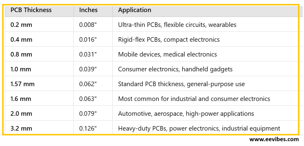
Here is a tabular representation of some commonly used PCB thickness standards across different applications:
Future Outlook and Challenges
Looking ahead, the PCB market’s trajectory suggests a continued balancing act between standardization and customization of thickness. The push for sustainability—evidenced by initiatives like the development of eco-friendly laminates (e.g., Soluboard)—may influence thickness standards as manufacturers seek lighter, recyclable materials to reduce environmental impact.
However, challenges such as supply chain disruptions, rising raw material costs, and the complexity of producing ultra-thin or ultra-thick boards could temper growth. Addressing these hurdles will require innovation in manufacturing techniques and collaboration across the value chain.
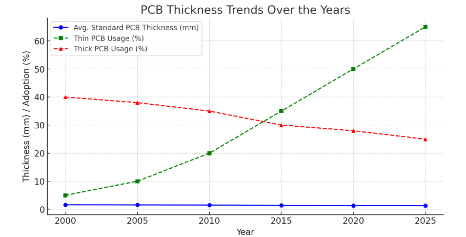
- The standard PCB thickness has been gradually decreasing from 1.6 mm to 1.3 mm due to miniaturization and efficiency improvements.
- The adoption of thin PCBs (≤0.8 mm) has significantly increased, especially in consumer electronics and wearables.
- The usage of thick PCBs (≥2.0 mm) in high-power and industrial applications has declined slightly but remains relevant.
In conclusion, standard PCB thickness remains a cornerstone of the industry, rooted in historical precedent yet adapting to modern demands.
As the market evolves—projected to exceed USD 113 billion by 2032 at a CAGR of 5.9%—thickness will continue to play a pivotal role in shaping design choices, manufacturing efficiency, and application suitability.
Whether catering to the sleek profiles of consumer electronics or the rugged needs of industrial systems, the interplay between standard and custom thicknesses reflects the dynamic nature of the PCB market, poised for sustained growth and innovation through the coming decade.