Introduction to logical effort
In this article I will explain logical effort and its examples. How it effects the speed of digital circuitry? The method of logical effort is a technique used to estimate the delay in a CMOS circuit, Now, what is a CMOS circuit. It is a combination of metal oxide semiconductors which are used to implement logic gates and other digital circuits. Logical effort simply can help select gates for a given function (including the number of steps required) and reduce the size of gates to reduce circuit delays.
“Logical effort is the ratio of the input capacitance of a gate to the input capacitance of an inverter delivering the same output current”.
Examples of calculating logical effort
- Electronic digital circuits are usually made from large combination of logic gates, often packaged in integrated circuits. Complex instruments can have a simple electronic representation of the functions of Boolean logic.
- Logical effort captures enough information about a logic gate’s arrangement in the circuit—the network of transistors that connect the gate’s output to the power supply and to ground—to determine the delay of the logic gate.
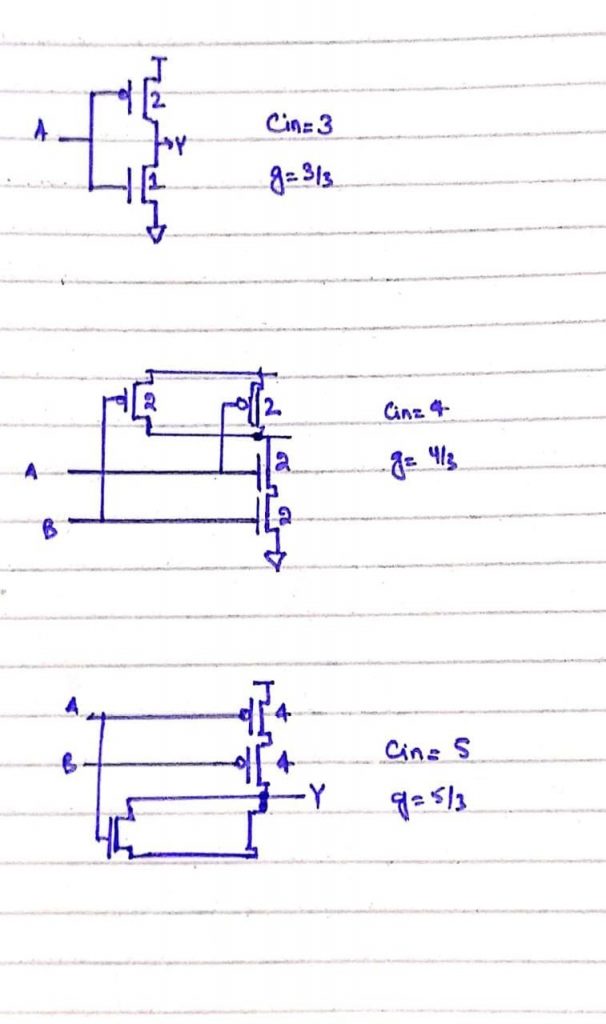
- The logical effort of a two-input NAND gate is calculated to be g = 4/3because a NAND gate with input capacitance 4 can drive the same current as the inverter can, with input capacitance 3. Similarly, the logical effort of a two-input NOR gate can be found to be g = 5/3.
Logical effort is a method to make following decisions
- Uses a simple model of delay
- Allows back-of-the-envelope calculations
- Helps make rapid comparisons between alternatives
- Emphasizes remarkable symmetries
Delay in a Logic Gate:
The delay is the length of time it takes for a signal to travel to its destination. In simpler, delay of a logic gate is defined as the time it takes for the effect of change in input to be visible at the output. In other words, delay is the time required for the input to be propagated to the output.
- Delay has two components
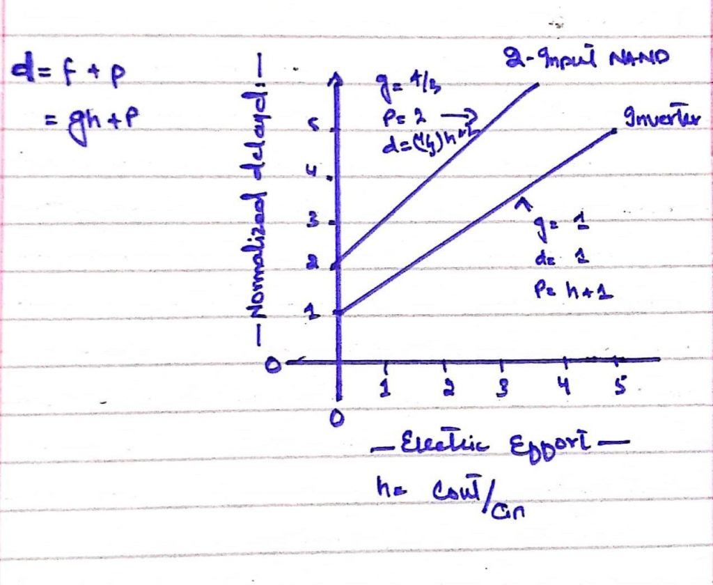
- d = f + p
where, p represents delay of gate driving no load set by internal parasitic capacitance.
Where ‘f’ is effort delay. f = gh. Again, effort delay has two components
- g: logical effort: measures relative ability of gate to deliver current. g ≡ 1 for inverter.
- h: electrical effort = Cout / Cin. Ratio of output to input capacitance, also called fanout.
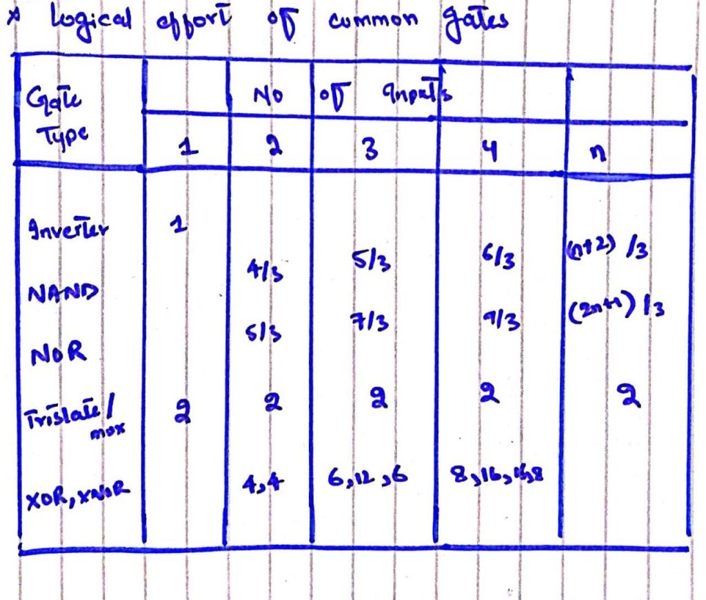
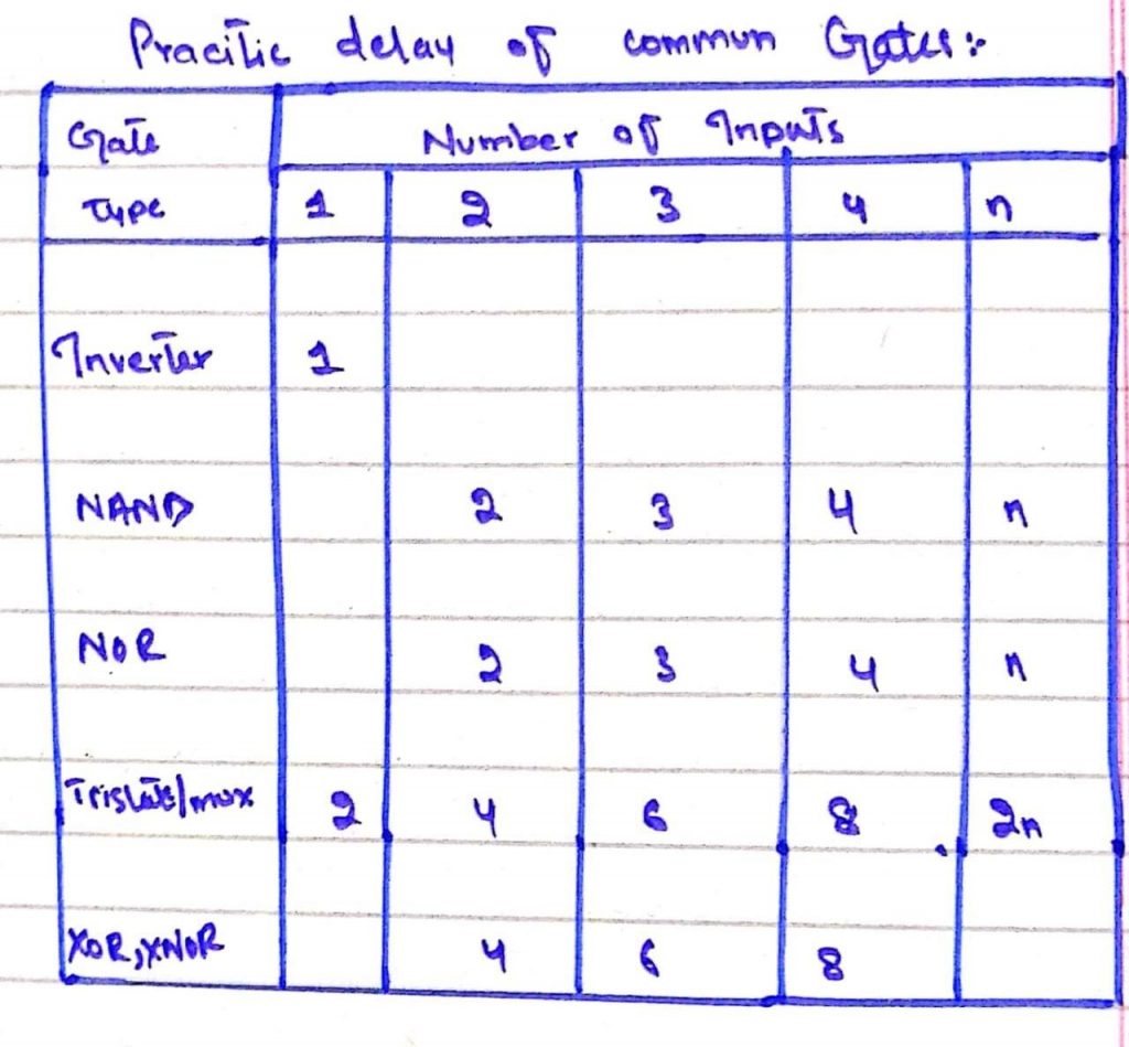
Catalog of Gates:
Reducing Number of Logic Stages:
- If we have too low EF, we will use more complex gates with fewer stages
- Often need to use AND OR-Invert gates or ORAND-Invert gates
Logical Effort “Design Flow”:
- Estimate the path effort
- Estimate the optimal number of stages
- Estimate the minimum delay
- Determine the actual number and type of gates – Fit the required logic in N stages, where N is close to N* – This may slightly change the path effort
- Determine the new stage effort
- Working from either end, determine gate sizes
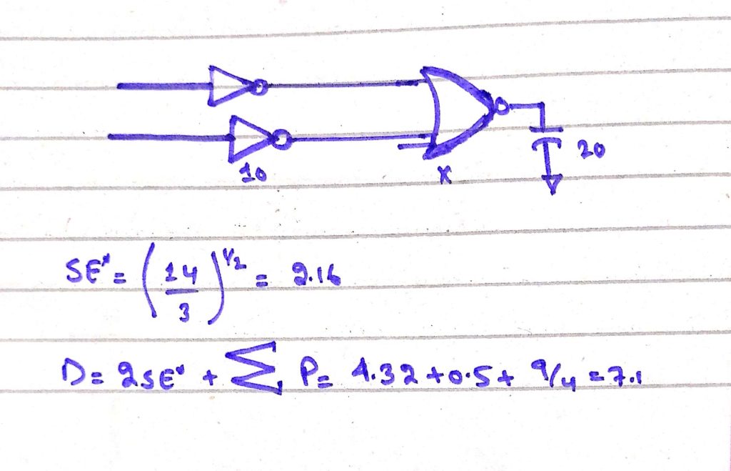
Effect on speed of logical effort on digital circuitry:
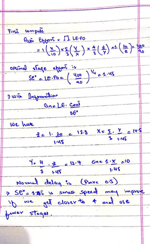
The normalized delay is (assuming Pin v=0.5)
D=4SE*+Sum Of P=4 1.45+ 0.5+ 1.5 +1+ 0.5= 9.3
- SE*=1.45 is small. Speed may improve if we get closer to 4 and use fewer stages.
Also read here
https://eevibes.com/digital-logic-design/what-is-the-programmable-logic-array-pla/