Abstract
What is VLSI IC technology and Y chart? The Computer Systems Laboratory participated in the VLSI research program for a year and a half. Major areas under investigation include: design and integration design tools, use of VLSI in computer graphics, workspace design, special purpose chip design, VLSI computer architecture, and hardware specifications and verification. Progress is being discussed on these research issues, and a research plan for the next two years is proposed.
Background
At the beginning of the 21st century, we were surrounded by a variety of machines and applications that could be built without the use of electronics.
In addition, the communications development that we now see would not be possible without advances in the electronics industry and the use of integrated circuits (ICS). The integrated circuit can easily be described as a large area built into a very small semiconductor chip. What started as a few transistors on a single chip in the early 1970’s has grown to one billion transistors over 40 years. The ever-increasing demand from humans has pushed the technology to combine multiple components into a single chip. And the trend is expected to continue.
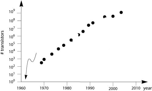
The emergence of Very Large-Scale Integration (VLSI) in the last half century is shown in Figure 1, as well as major events. In terms of the integration of components into a single death, IC technology is divided into several stages, of which VLSI is an advanced integration level. The term VLSI is used in connection with the construction and construction of integrated circuits (ICs).
IC Technology
VLSI technology has contributed to the development of the current era of electronic and communication devices. Silicon has become a natural choice for the production of composite circuits due to its rich properties and most importantly its native oxide which is best suited to produce composite circuits. About 90% of the world’s electrical circuits are made of silicon as a result of CMOS technology. CMOS technology is the most popular technology due to its low power and small space. Lets discuss now VLSI IC technology and Y chart.
Methodology
Very Large Scale Integration (VLSI) is a process of creating an integrated circuit (IC) by combining thousands of transistors into a single microcircuit. VLSI began to develop advanced semiconductors and communication technologies in the 1970s. The microprocessor is a VLSI device. Prior to the advent of VLSI technology, the performance of multiple integrated circuits was limited. Electronic circuits may include processors, ROMs, RAM, and other logical related components. VLSI allows integrated circuit designers to add all of these to one chip. The electronics industry has grown exponentially in the last few decades, largely due to rapid development in a large area.
Integrated measurement technology and system design applications. With the advent of Very Large Scale Integration (VLSI) projects, the use of integrated circuit (IC) is rapidly increasing in high computer performance, control, telecommunications, image and video processing, and other household appliances. I am. Modern advanced technologies such as high resolution, low bitrate video, and mobile connectivity provide end users with an amazing amount of applications, processing power, and portability. This trend is expected to grow rapidly and have a significant impact on VLSI construction and system building.
The VLSI IC circuits design flow
The flow of the VLSI IC circuit is proven within the parent below. Many sections of a building have numbers and blocks that show tricks within the slide of the building. Details come first, clearly defining the functionality, functionality, interface, and design of the visual IC circuit to be designed.
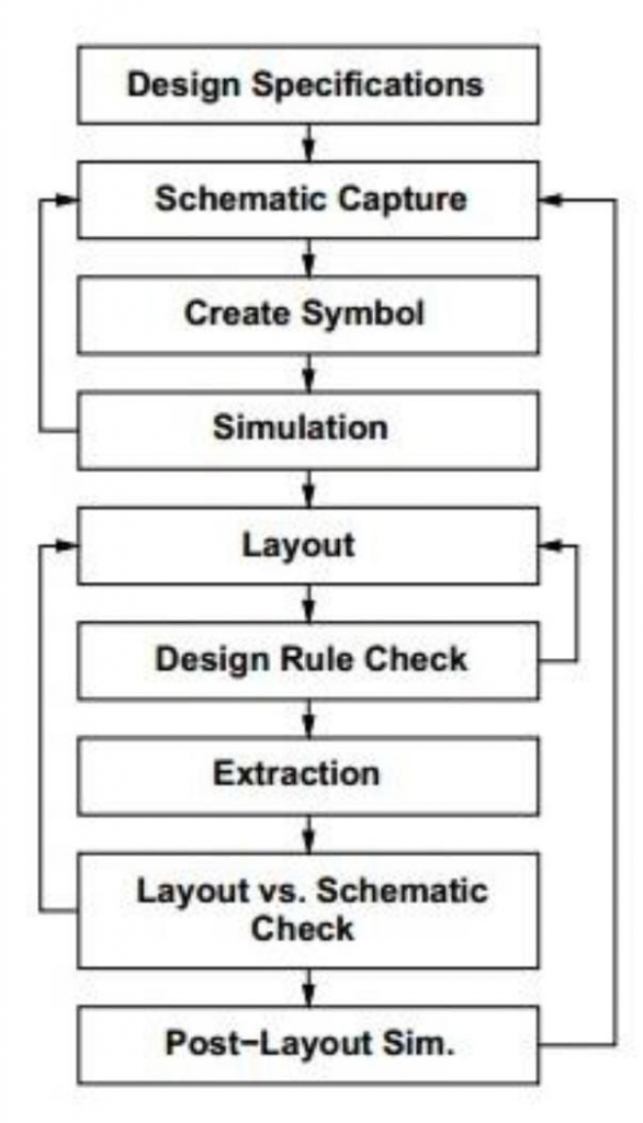
Definition of behavior has been created to analyze the design in terms of performance, functionality, compliance with specific standards, etc. specified RTL definition is created using HDL. This RTL definition has been modified for performance testing. From here on out we need the help of EDA tools. The definition of RTL is then converted to a gate net list using sensible integration tools. A gate-level net list is a description of the circuit in terms of the gates and the connections between them, which are made in such a way that they meet time, power and location details
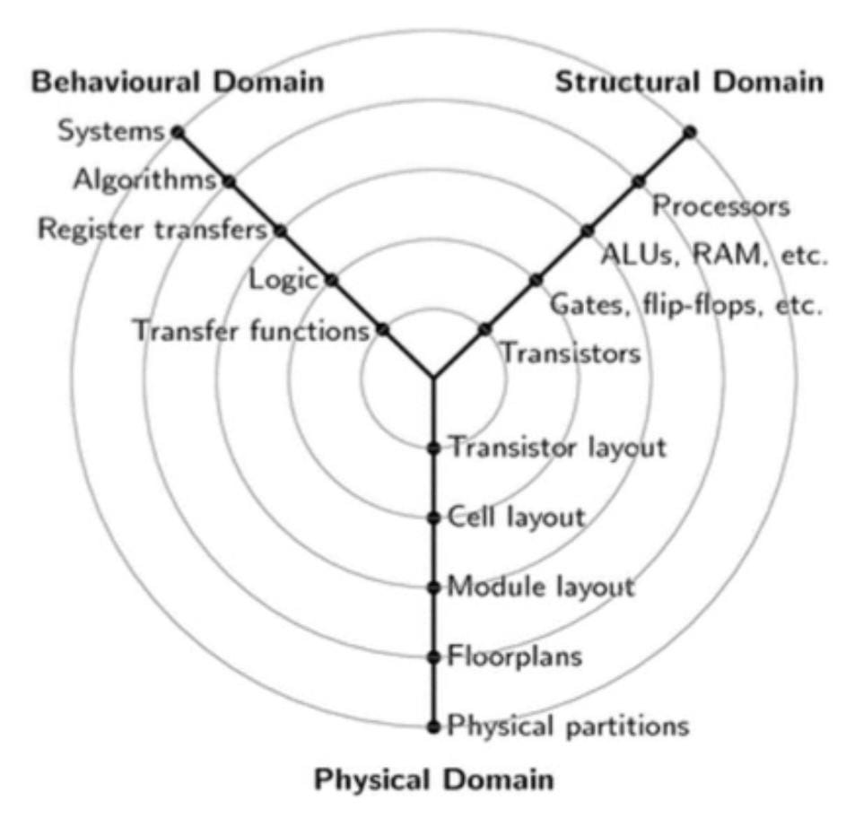
What is Y-chart?
VLSI IC technology and Y chart Y-chart Gajski Kuhn Y chart is a model that writes considerations in the construction of semiconductor devices. Three Gajski Kuhn Y chart domains lie on the radial axes. Each field can be divided into output levels, using fixed rings. At the top level (outer ring) we look at the chip design; at lower levels (internal loop) we sift the design sequence into a more detailed implementation – Producing a structure definition from a descriptive character is done using high-quality integration processes or logical integration.
.
Design Hierarchy-Structural
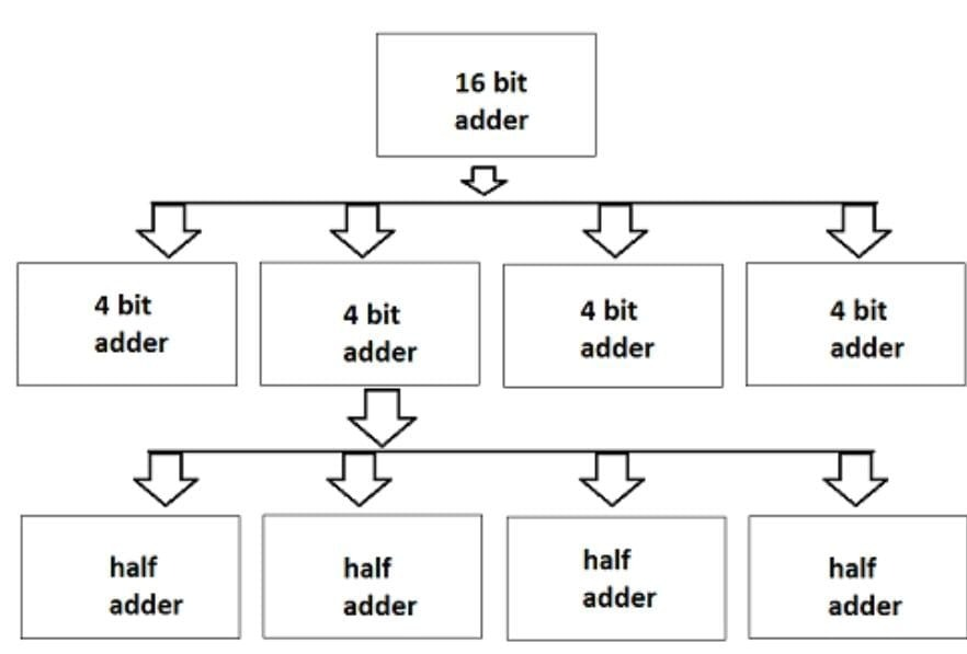
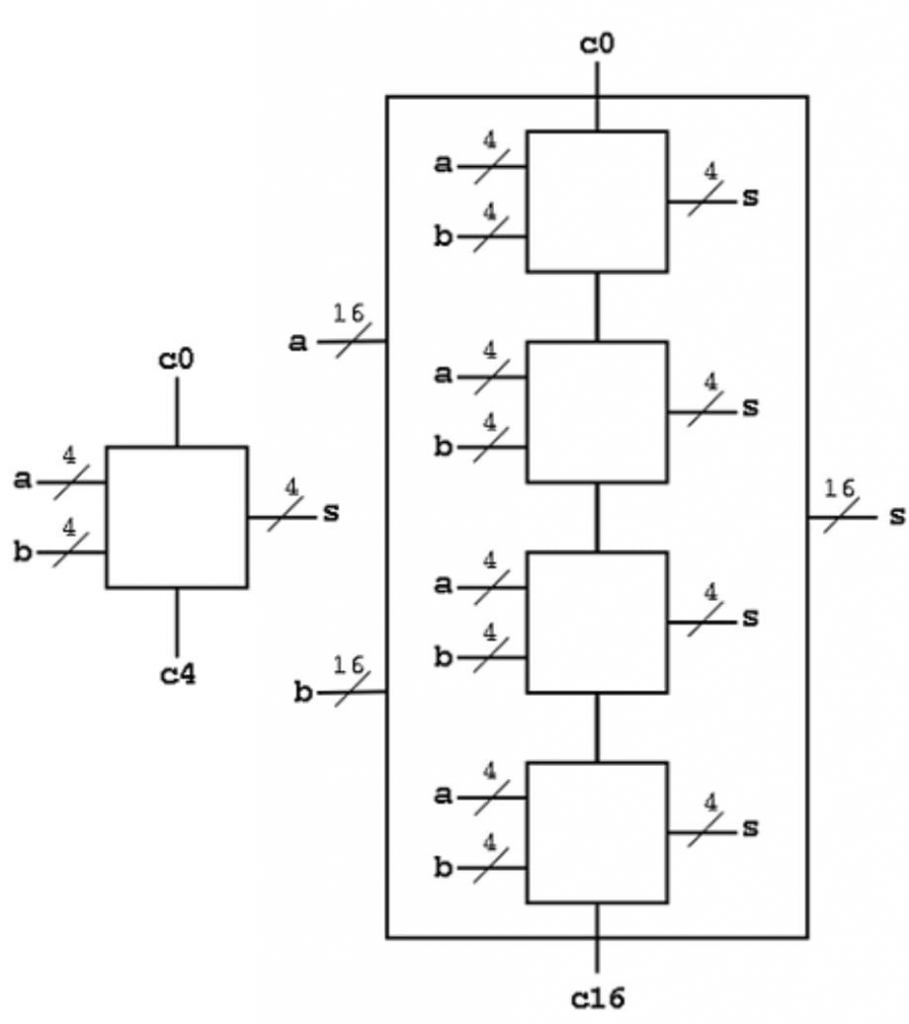
Here, every 16 bit adder chip is divided into four 4-bit adder modules. Additionally, split 4 adders into 1-bit adder or half adder. The addition of 1 bit is an easy design process and its internal rotation is also easy to do on the chip. Now, connecting all the last four adders, we can design 4 adders and move on, we can design a 16-bit adder.
Timing analysis in VLSI circuits
In virtual VLSI circuits, it’s miles vital to decide an upper restrict on the remove of all paths from the primary inputs to the number one outputs. Statistical Timing Analysis (STA) is one of the conventional simulation procedures to characterize the timing overall performance of virtual circuits, to decide the important paths, and to obtain the put off statistics. It is an exhaustive approach of studying, debugging and validating the timing ordinary overall performance of a layout. A conventional STA tool breaks down the whole design into timing paths, calculates the postpone on every route with the aid of way of estimating the inter-cell and intra-cellular delays and then assessments for violations of timing constraints on every path.
Conclusion
The intent of the experiment was familiarization VLSI Electric and Win spice. The design of VLSI electronic circuits can be achieved at many different abstraction levels, Where in each level represents a different model of the same information and processes, but with varying amounts of detail, starting from system behavior to the most detailed, physical layout level. The Electric VLSI Design System is an open-source Electronic Design Automation system that can hand le many forms of circuit design, including Custom IC layout, digital and Capture, Textual Languages such as VHDL and Verilog, etc. Electric also provides an excellent way of integrating different environments of design.
Future work
Starting from your far off of television, washing device, mobile cell phone, microwave oven, AC, Car electronics, Space ships, aviation, weather forecast, satellites, defense everywhere these days, electronics has penetrated. The digitization race has asked every day for modern day digital systems having low electricity intake, higher battery backup, low cost, fastest computational pace, and very quick format time. For those demands to suit up electronics are shrinking and shrinking. The observe that is answerable for designing those forms of electronics is referred to as at gross, very large scale integration. Widely named as VLSI. If VLSI engineers are not sparing day and night time for those miniaturization the betterment of electronics and signaling systems will save you. So for masses coming years VLSI could be at boom. I advocate youngsters to sharpen their expertise in VLSI.A lot is coming up men, particularly even as India is pledging to end up Aatmnirbhar. The Modi’s government is sincerely considering growing the foundries for chip manufacturing. If the foundries begin, the dependency on distinctive nations for mobile cell phone and computer processor chips will reduce. I also suggest you to sign up for the telegram company VLSI Chaps for cutting-edge problem updates and interactions.
Also read here
What are the sequential programmable devices? Discuss any of them in detail