Introduction to Computer Aided Engineering Tools
4 Layer PCB Fabrication and Design Steps. Before going into the details of designing layout, let us first get the idea what are the computer aided engineering (CAE) tools. All the aspects from drawing to analyzing to manufacturing are covered in CAE tools. One of the categories of CAE is Computer Aided Design (CAD) which is related to the physical layout of digital system design. All the CAD programs that are linked specifically to electronics industry are known as Electronic CAD or EDA (electronic Design Automation).
Development time and cost are reduced because of EDA tools since they allow to simulate and analyze design before they are purchased or manufactured on hardware. Once you are done with the drawings, simulations and analysis, the system can be manufactured. Applications that are used in manufacturing are known as computer-aided manufacturing or CAM. In order to bring a design concept into reality, software programs and design data are used by the CAM.
A mathematical model is contained in PSpice (which is a CAE tool) for performing simulations. For converting a symbolic schematic diagram into physical representation of a design, we use layout which is actually a CAD tool. In addition to that layout is also used as front end CAM tool. It does that by generating the data on which other CAM tools operate when you design a printed circuit board (PCB). For interconnecting parts within a design we use netlist. Netlist is also used for connecting each of the parts with its model and footprint.
If you consider to combine all these three applications into one package, then you can have a very powerful tool for testing, designing and building electronic circuits. For designing a successful project you need to understand these tools and a PCB itself.
Empowering innovation, Rush PCB Inc stands as your trusted partner in delivering high-quality, custom PCB solutions.
Printed Circuit Board Fabrication
Now lets see how can we fabricate PCB so that we can have better understanding of how to use CAD tools and layout. Two basic parts of a PCB are:
- a substrate which is actually a board
- and printed wires that are actually copper traces.
Substrate provides a structure where you will physically place the components and copper traces provides insulations between the conductive paths.
FR4 is the common type of substrate and it is known as fiber-glass-epoxy laminate. This resembles to older fiberglass boards but it is flame resistant. Others materials that can be used for making substrate are: Teflon, ceramics, and special polymers.
Also check
Learn How many types of Printed Circuit Boards are manufactured?
Steps Involved in Fabrication and Design of 4-layer PCB
Following steps are involved in the fabrication and design process of a 4-layered PCB. Let us discuss each of them individually.
Front-end Tool Data Preparation
The board designer has prepared his layout on a computer aided design (CAD) system. Each CAD system uses its own internal data format so the PCB industry has developed a standard output format to transfer the layout data to the manufacturer. This is extended Gerber or rs-274x. The Gerber files define the copper tracking layers four in the job we are following as well as the solder marks and components notations.
First we check that data meets our manufacturing requirements. These checks are mostly done automatically. We check the track widths, the space between the tracks, the pads around the holes and the smallest hole size etc.

The engineer can also check and measure individual areas where he wishes. Once the data is verified as good he will output all the tool files needed to drive the machines that will make and test the PCB.
Preparing the Photo-tools
We use laser photo plotters in a temperature and humidity control darkroom to make the films we will use later to image the PCBs. The photoplotter takes the board data and converts it into a pixel image.
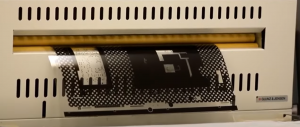
A laser writes this onto the film. The exposed film is automatically developed and unloaded for the operator. We have generated one film or photo tool per PCB layer.
Now the films are registered with each other so that the different layers of the PCB will be perfectly aligned.
We do this by punching precise registration holes in each sheet of film.
The operator puts the film on the table of the punch and then micro adjust the table until the targets on the film are exactly lined up with the targets on the film punch.
Operator then punches each sheet of film with the registration holes which will fit into the registration pins in our imaging equipment.
Print Inner Layers
To produce the inner layers of our multi-layer PCB we start with the panel of laminations. Laminate is an epoxy resin and glass fiber core with copper foil pre-bonded onto each side. The first step is to clean the copper.
We print the panels in a clean room to make sure that no dust gets on to the surface where it could cause a short or open circuit on the finished PCB.
The clean panel is coated with a layer of photosensitive film. The photoresist the bed of the printer has registration pins matching the holes on the photo tolls and in the panel. The operator loads first film on to the pins then the coated panel then the second film.
The pins ensures that the top and bottom layer are precisely aligned. The printer uses powerful UV lamps which harden the photo resist. through the clear film to define the copper pattern. Under the black areas the resist remains unhardened. The clean room uses yellow lighting as the photoresist is sensitive to UV light.
Outside the yellow room the panel is sprayed with a powerful alkali solution which removes the unhardened resist.
The panel is pressure washed and dried. The copper panel we want is now covered by the hardened resist.
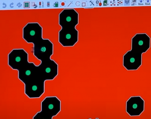
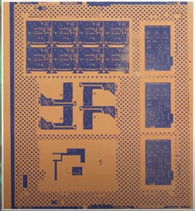
The operator checks a sample of the panels to make sure that the copper surface is clean and all the unwanted resist has been removed. You can now see in the blue resist what will be the copper on our inner layer as shown in the figure below.
Etch Inner Layers
Unwanted copper layer is removed using a powerful alkaline solution to dissolve or etch away the exposed copper. The process is carefully controlled to ensure that the finished conductor widths are exactly as designed. But the designer should be aware that thicker copper foils need wider spaces between the tracks.
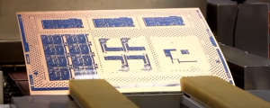
The operator check carefully that all the unwanted copper has been etched away. Next we strip the blue photo resist which protected the copper image so now we have the exact pattern required. The operator check the older photo resist has been removed. You can see that euro circuits put several designs on one production panel. That way we can make small numbers of PCBs cost effectively.
Register Punch and Automatic Optical Inspection (AOI)
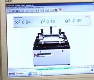
The inner-core of our multilayer is now complete, next we punch the registration holes we will use to design the inner layers to the outer layers. The operator loads the core into the optical punch which lines up the registration targets in the copper pattern and punches the registration holes.
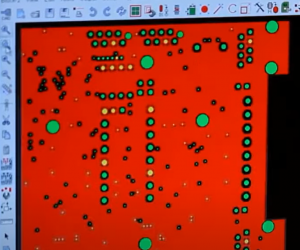
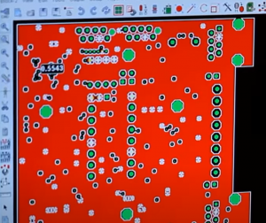
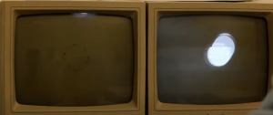
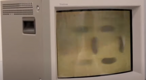
We will not be able to correct any mistakes on the inner layers once we have assembled the multilayers. So we now give the panel a complete machine inspection. The automatic optical inspection system scans the board in broad strips and compares it with the digital image generated from the original design data. any errors present are displayed on the screen as shown below.
Lay-up and Bond
The outer layers of our multilayer consist of sheets of glass cloth pre-impregnated with uncured epoxy resin or pre-peg and a thin copper foil. The lay-up operator has already placed a copper foil and two sheets of pre-peg on the heavy steel base plate. Now he places the pre-treated core carefully over the alignment pins. Then he adds two more sheets of pre-peg another copper foil and an aluminum press plate.
he builds up three panels on the base plate in the same way. He then rolls the heavy stack under a press which lowers down the steel top plate. He pins the stack together and rolls the finished stack out of the clean room into a rack.
The press operator collects three stack on a loader and loads them into the bonding press. This press uses heated press plates and pressures to bond the layers of the PCB together. The heat melts and cures the epoxy resin in the pre-peg while the pressure bonds the PCB together. Pressure is computer controlled to build up the heat and the pressure correctly hold it and then to cool the press down.
In this way we ensure a permanent bond that will last the lifetime of the PCB. This board that we have designed have four layers but complex PCBs for defense avionic and telecommunication applications can have more than fifty. These may include sub-assemblies of cores, pre-pegs and foils drilled and plated before being assembled into the final PCB.
Once the cycle is completed, the press operator unloads the press and carefully rolls the heavy stacks into the clean room. Here the layup operator d-pins the stack and removes the top plate. He unloads each of the panels from the stack. Removing the aluminum press plates used to ensure a smooth copper finish. The copper foil is now bonded in place to form the outer layer of PCB.