Introduction to small signal amplifiers
what are the small signal amplifiers and their applications? The word amplify means some device that can “increase”. So amplifiers are the circuits that are used to increase the magnitude of voltage or current.
What is the meaning of small signal amplifiers?
Small signal name is given as they amplify the input signals that are very small in magnitude usually in mV. While designing the amplifiers, you need to make sure of two things:
- Biasing point (operating point)
- Biasing configuration (common emitter, common base, and common collector)
The biasing point of an amplifier actually decides to determine the shape of output signal and the biasing configuration helps to determine the phase of output signal, type of gain, and input/output impedance. Transistors are used for designing amplifiers and the most widely used transistors for that are bipolar junction transistors. If you generally discuss the biasing point or operating point of a transistor you can say that it’s the point that is set with dc biasing. For understanding the operating point of a transistor, have a look of transistor characteristics curves. The following figure shows the characteristics curve of a transistor.
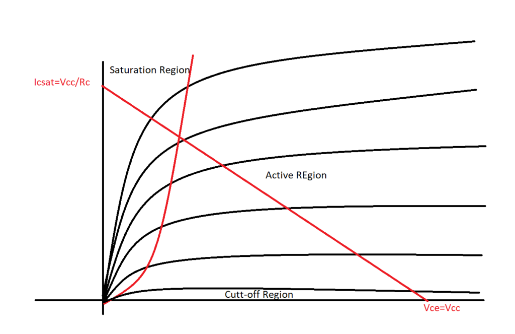
Regions of operations of small signal amplifiers.
Three regions have been identified: cut-off region, linear region, and the saturation region. Let’s have brief description of each.
1. Cut-off region
In this region the transistor is said to be in non-conducting mode. Here, a very small leakage current flows through it and we can say transistor is in OFF state. In this case output voltage is equal to the supply voltages () and output current is zero (approximately).
2. Linear region
Whenever we say transistor is in its linear region means it is under normal operating conditions. In this region we actually perform the amplification process. When the transistor is biased such that it will have the operating point in the middle of the curves and the amplification will be linear. In this case it has some non-zero value of output voltage and output current.
3. Saturation region
When both junctions of the transistor are forward biased, the transistor is said to be operating in the saturation region. In this region, maximum output current flows through the transistor and the output voltage is approximately equal to zero (ideally) or 0.02V (practically). In this region transistor is said to be in ON state.
Now, once you are familiar with these three regions of a transistor you can decide in which region you should operate the transistor. If the transistor is biased such that it operates in the saturation and cut-off region then it can be used to design a switch/inverter from it.
Transistor as an inverter
One of the most widely used application of the transistor is an inverter. Means it can invert the input voltages. The following figure shows how we can configure the transistor as an inverter. When the input voltages is equal to zero (0 logic) then the input current is also zero, causing no output current and hence there will be no voltage drop across the resistor. The output voltages will be equal to Vcc (logic 1).
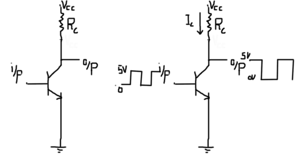
When we apply some input signal which causes some to flow results in some output current . This output current is the maximum current according to the given source which results maximum voltage drop across the resistor. Hence the output voltage is equal to 0 or 0.02v.
Concluding our discussion, we can say that when input is low, output is high and when input is high, output is low. In this way transistor acts as an inverter or a switch.
Types of Amplifiers
Three types of the amplifiers are designed based on the fact that which of the terminals is kept common. That are:
- Common Emitter (CE)
- Common Collector (CC)
-
Common Base (CB)
Common Emitter (CE):
The common emitter amplifier provides both types of gains (voltage and current). It has low input resistance because the input side is actually a Base-Emitter junction and hence a very small resistance it has. The output resistance of CE amplifier is very high because the Collector-Base junction is the output side which is usually reverse biased. Another property of common emitter amplifier is that it gives inverted output i.e., 180 degree out of phase of the input signal. Its the most widely used amplifier because it provides both types of gain.
Common Collector (CC) :
Another name of common collector amplifier is the emitter follower. That is, the output follows the input because its voltage gain is approximately equal to unity. It only provides the current gain. It has high input resistance that’s why it can be used for matching the impedance. Its current gain is approximately equal to the gain (Beta) of the transistor.
Common Base (CB):
It is rarely used amplifier as it only provides the voltage gain. The current gain achieved through this amplifier is approximately equal to one.
Which configuration is better? common emitter, common base or common collector?
Common emitter configuration is better as it provides both the voltage and current gain.
Q point is more stable since it is independent of beta.
The characteristic curves are easy to understand pus they have normal behavior.
Also read here :
https://eevibes.com/what-are-the-basics-of-operational-amplifier/
What are the basics of operational amplifier? Why do we use operational amplifier (op-amp) ?