Table of Contents
Introduction to Power Dissipation in Logic Gates
How the Power is Dissipated in Logic Gates? The amount of electric power dissipated by the transistors in an electric circuits is important to be considered. This is because of the fact that million of transistors are fabricated on a single chip. That is why power consumed by a single transistor on a chip is important and must be small. In all logical circuit applications, power dissipation is an important consideration. It becomes crucial when we talk about battery operated circuits or devices for example portable laptops and tablets.
Example
Consider the following NMOS NOT gate. When input voltage Vx=0, then no current flows through the circuit and hence no power is consumed.
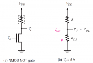
But when we apply input voltages Vx=5V, then steady state current Is will flow through the transistor and hence the dissipated power is given as the product of steady state current Is and biased voltages VDD, P=Is.VDD.
Now if we assume that a chip contains 10,000 inverters then the power consumed in total is 10W. Because of this high power consumption, NMOS based inverters are used in only special purpose applications.
In order to differentiate between the power consumed by when the signals are changing and power consumed during steady state, it is necessary to define there are two types of powers:
- Static Power
- Dynamic Power
Static Power
This power is dissipated because of the flow of current during steady state conditions. Dynamic power is dissipated when the signal changes its level.
Both static and dynamic power is dissipated by NMOS circuits while in case of CMOS circuits, only dynamic power is consumed.
Read here about
What are the CMOS Logic Gates?
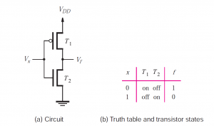
Now, consider the CMOS realization of NOT gate as shown in the figure below. When the input voltage Vx=0V, no current will flow as NMOS transistor is OFF. Similarly, when Vx=5V (high) there will be no current again because PMOS transistor is OFF. In short, in steady-state there is no current flowing. The current will only flow for a short span of time in the case when one voltage level is switched to another level.
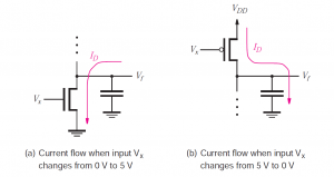
Let us consider another case as depicted in the following figure. When Vx=0V for some time then Vf=5V. Now if you make Vx=0V, NMOS transistor turns ON and it will result to pull Vf=0V (GND). Because of the presence of Parasitic Capacitance at the node f, Vf does not switch its state instantaneously. Drain current flows for a short period of time through the NMOS transistor while capacitor discharges. The same situation happens when Vx changes from 5V to 0V as shown in part b of the following figure. In this case capacitor has initially 0V across it and then it charges to 5v through PMOS transistor. Current takes path from power supply to PMOS transistor to charge the capacitor.
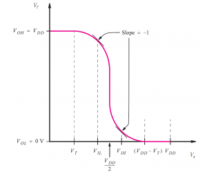
Voltage transfer characteristic for the CMOS inverter
The voltage transfer characteristic for the CMOS inverter is shown in the figure below. These characteristics show that there is a range of input voltage Vx for which both transistors are turned ON. Current will flow from VDD to GND within this voltage range VT < Vx < (VDD − VT ) through both transistors. This current is usually referred to as short circuit current of the gate and it is quite negligible as compared to the current that actually (dis)charges the capacitor.
A single CMOS transistor uses very small amount of power. Consider the case when Vf=VDD. The capacitor stores energy equal to the amount of CVDD2/2. During the discharging of capacitor, this stored energy is dissipated in NMOS transistor is depicted in Figure 3(a). Similarly, during the charging of capacitor, the same amount of energy is dissipated in PMOS transistor. Hence in complete cycle of charging and discharging, the total amount of dissipated energy is CVDD2. Since Power is equal to energy used per unit of time, the dissipated power in an inverter is the product of energy used in one charging or discharging cycle times the number of such cycles per second, f . Hence we can calculate the dynamic power used as:
PD=fCVDD2
Practically, total dynamic power used by CMOS inverter is small as compared to the power consumed by any other technologies like NMOS technology. This is the main reason all larger integrated circuits prefer to use CMOS technology.
Also read here