Discuss the MOSFET fabrication and Behavior in detail. In order to get the idea of how NMOS and PMOS transistors work, we need to learn how they are designed as an integrated circuits. Silicon wafers are used for fabricating the integrated circuits.
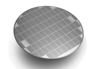
The diameter of silicon wafer is usually 6,8 or 12 inches and usually it resembles to compact disk (CD) in shape. A single wafer is used for fabricating many chips and then that wafer is cut for getting an individual chip.
Silicon is actually a semiconductor material which usually do not conduct under normal conditions. Conduction can take place under special conditions. A transistor is fabricated by adding purities in the substrate such that one part of the layer has excess of either positive or negative charges. Negatively charged region is called the n-type region and positively charged region is named as p-type region. The structure of NMOS transistor is shown in the figure below.
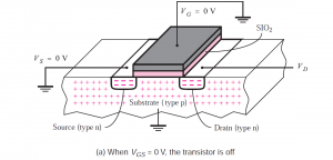
n-type silicon is used for both source and drain terminals and p-type material is used for substrate terminal. In order to make connections between source and drain, metal wiring is used.
Initially metal was used for drain terminal when MOSFET was discovered. But now polysilicon is used for this purpose. It is also conductor like a metal but it allows the fabrication to be done on very small dimensions. There is a layer of SiO2 that isolates the gate from the rest of the transistor.
When we apply the voltages across the terminals of the transistor, there is an electric field which determines the operation of transistor. The voltages at the terminals of transistor are referred to as VG, VS, and VD.
When (VG, =VS =0) then drain and source are isolated from each other by p-type substrate. In terms of diodes, we can say that there are two diodes between source and drain terminal. One results in p-n junction between drain and substrate and other is between source and substrate. Tis back to back arrangement results in very high resistance i .e., of the order of 1012 Ω. This much high resistance prevents current between drain and source terminals. So, in this case transistor is in cut off state or in turned off condition.
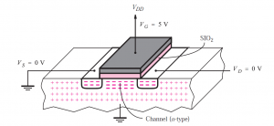
Now let us consider a case where we start increasing the voltages at the gate terminal with respect to the source. These voltages are referred to as VGS voltages. If these gate to source voltages are increased to a certain level called the threshold voltages, the transistor starts going into closed switch state from and open switch state. There are many factors that determine the value of VT but usually they are considered equal to 0.2VDD.
Formation of channel in MOSFETs
When we apply VGS=5v, it attracts the electron from n-type towards the gate terminal. Since these electrons can not cross the class insulation so they all are gathered in the region of substrate between gate and source terminal. This results in a channel. The size of this channel is dependent on the dimensions of the gate between source and drain. You can also consider the channel as a depth between source and drain. This depth is totally dependent on the voltages applied at drain, source and gate terminals.
There is no current from the gate terminal as it is isolated from the substrate. The only current that may flow is through drain to source and its value depends on the VDS by keeping VGS equal to constant.
When we keep VGS constant, drain current increases linearly with VDD. When VGD> VT then transistor is aid to be operated in triode region which is also called the linear region. The voltages and current are related as:
\begin{equation}
I_{D}=k_{n}^{\prime} \frac{W}{L}\left[\left(V_{G S}-V_{T}\right) V_{D S}-\frac{1}{2} V_{D S}^{2}\right]
\end{equation}
where kn’ is called the process transconductance parameter. The value of this constant depends on the technology we actually use. Its units are equal to A/V2
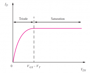
As we increase the value of VD the current increases and reaches to its maximum value when VDS=VGS-VT. On further increase in VDS ,transistor no longer operates in the triode region. Since at this moment it conducts the maximum current. At this point we say that transistor is operating in the saturation region and current becomes independent of VDS and it is equal to:
\begin{equation}
I_{D}=\frac{1}{2} k_{n}^{\prime} \frac{W}{L}\left(V_{G S}-V_{T}\right)^{2}
\end{equation}
Voltage and current relationship for NMOS transistor
The following figure shows the relationship between voltage and current for an NMOS transistor. This graph represents data for some fixed of VGS> VT. Th figure clearly shows the point (VGS-VT) at which transistor switches from the triode region to saturation region.
Also read here