Introduction to CMOS Technology
What are the CMOS Logic Gates? In CMOS technology, both NMOS and PMOS transistors are connected together for implementing the logic gates. In this article you will get the idea CMOS technology has many better advantages as compared to NMOS technology.
Logic functions in NMOS circuits are implemented using NMOS transistors that are combined with pull up resistors. The part of circuits that consists of NMOS transistor is called the pull down network (PDN).
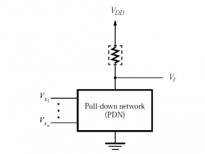

In CMOS circuits, pull up device is replaced with a pull up network (PUN) which is designed using PMOS transistor. This arrangement should be such that the circuits implemented by PDN and PUN should be the complement of each other.
For any given input value PDN pulls Vf down to Ground (GND) or PUN pulls up Vf to VDD. The number of transistors in PDN and PUN network are equal. They are arranged such that the two networks are dual of one another. Whenever the PUN has PMOS transistors in series, the PDN has NMOS transistors in parallel and vice versa.
Example of CMOS circuit: NOT gate
NOT gate is the simplest example of CMOS circuit.
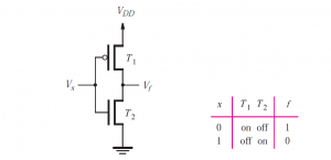
When Vx = 0 V, transistor T2 is off and transistor T1 is ON. This makes Vf = 5 V, and since T2 is off, no current flows through the transistors. When Vx = 5 V, T2 is ON and T1 is off. Thus Vf = 0 V, and no current flows because T1 is off.
The important point that you should always keep in mind is no current flows through CMOS inverter when the input is low or high. This is true for all COMS circuits that under steady state conditions, no current flows through the circuit and hence no power is dissipated. Because of this property. CMOS have become the most popular technology for designing the digital circuits.
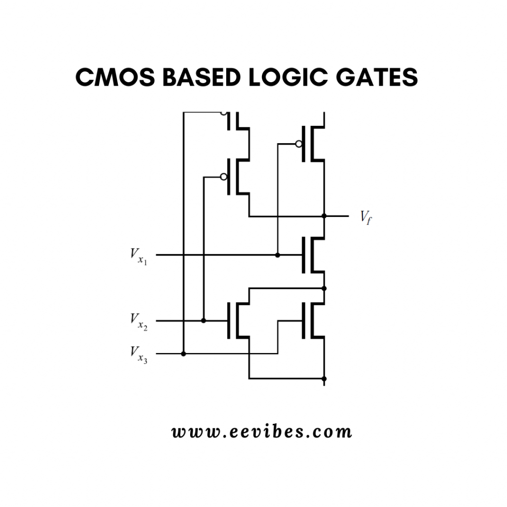
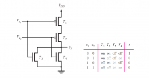
CMOS realization of NAND gate
The following figure shows the CMOS realization of NAND gate with its truth table.
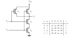
The truth table shows the logical states of each transistor corresponding to the different values of input x1 and x2. The NAND gate operation can be verified easily. Under static condition, there is no path for current between GND and VDD.
The circuit in above figure can be derived from the logic expression that defines the NAND operation, f = (x1x2)’. This expression specifies the conditions for which f = 1; hence it defines the PUN. Since the PUN consists of PMOS transistors, which are turned on when their control (gate) inputs are set to 0, an input variable xi turns on a transistor if xi = 0. From De Morgan’s law , we have
\begin{equation}
f=\overline{x_{1} x_{2}}=\bar{x}_{1}+\bar{x}_{2}
\end{equation}
So, f=1 whenever any of the inputs is equal to 0 which implies that there must be two PMOS transistors in parallel inside the PUN. The PDN on the other site must implement its complement. That is
f’=x1x2
Since f=1 only when both inputs are equal to 1. This means that there must be two NMOS transistors in PDN connected in series.
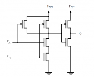
CMOS realization for NOR gate
The CMOS NOR gate circuit is derived from the following NOR gate expression that defines the operation of NOR gate.
\begin{equation}
f=\overline{x_{1}+x_{2}}=\bar{x}_{1} \bar{x}_{2}
\end{equation}
Here the function value is equal to 1 only when both inputs are equal to 0. This implies the PUN consists of two PMOS transistors that are connected in series. On the other hand PDN has two NMOS transistors connected in parallel. This results in the following circuit
CMOS realization of AND gate
So far you have learnt about the basic gates using CMOS technology, now you can generalize this concept for rest of the logic gates. A CMOS based AND gate is designed by placing a NOT gate before the NAND gate. Similarly, an OR gate is designed by putting a NOT gate before the NOR gate.
Also read here
- How to design a 4 bit magnitude comparator circuit? Explanation with examples
- What is the magnitude comparator circuit? Design a 3 bit magnitude comparator circuit
- What are the synchronous counters? Explain with an example.
- what are the half adder and full adder circuits?
- what are the half subtractor and full subtractor circuits?
- How to design a four bit adder-subtractor circuit?
- What are number systems in computer?
- Discuss the binary counter with parallel load? Explain its working with an example
- how to draw state diagram of sequential circuit?
- How to simplify a Boolean function using Karnaugh map (k-map)?
- What are the flip flops and registers in digital design?
- Define fan-in, fan-out, CMOS and TTL logic levels
- what is the Canonical form representation of Boolean function?
- What is difference between latches and flip flops?