Introduction to Tunnel diode
How Tunnel diode works? By increasing the impurities level in a simple diode, we can change its VI characteristics drastically. The characteristics curve exhibits a special property called the negative resistance region whose application can be seen at microwave frequency.In a general purpose diode, the doping level is 1 in 108. If this is increased to 1 in 103 then tunneling phenomenon takes place.
The thickness of the depletion layer is also reduced almost to 10-6 cm with the increase in doping level. This is 1/5thof the wavelength of visible light. With this thin depletion layer tunneling takes place. Such types of diodes are called Tunnel diode or Esaki diode. The charge carrier must possess the amount of energy that is required for crossing the barrier potential. However when the depletion layer is thin enough then charges will penetrate through it.
How Tunnel diode works?
In order to understand the working of Tunnel diode we need to study the energy-band diagram that is shown below.
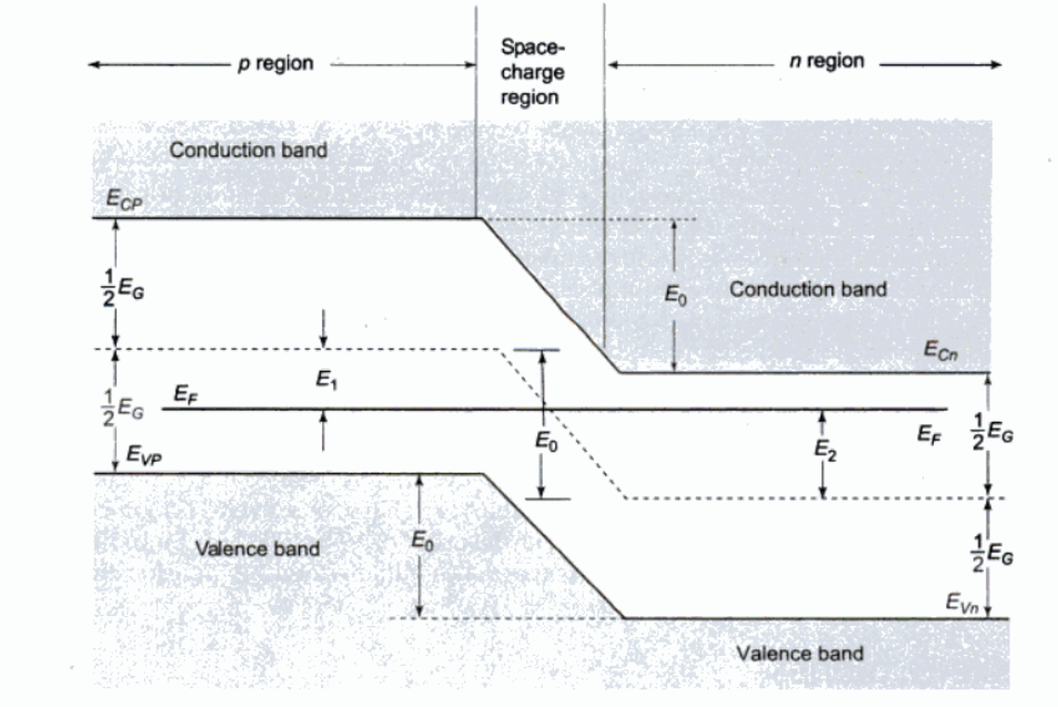
The energy state with the 50% probability of being filled with no forbidden band is known as the fermi level. For an intrinsic semiconductor material the fermi level lies in between the valence band and conduction band. When we add the impurities, this level shifts up or down. If the material is of p-type, the fermi level shifts towards the valence band and will be just above the valence band. If the material is n-type, then this will be up the conduction band.
Energy band diagram of tunnel diode
The above figure shows the energy band diagram of Tunnel diode. It can be seen in the above figure(a) the fermi level is not in the forbidden energy gap now. It has been pushed to valence band and now is in the conduction band of n-region. If the diode is open circuited, then the fermi level will be same in both regions. In the p-region we can see an empty space above the fermi level in valence band where electrons can exist. But in the n region valence band is completely full. There are electrons in conduction band of n-region and p-region that are of same energy level in this diode. As the depletion layer is so thin, so these electrons in the conduction band of n-region can penetrate to reach into the p-region. Similarly the electrons in the p-region that possess more energy as compared to the electrons in the conduction band of n-region will move into n-region. So, the electrons will move by maintaining equilibrium in both regions but in opposite direction thus causing zero current in it.
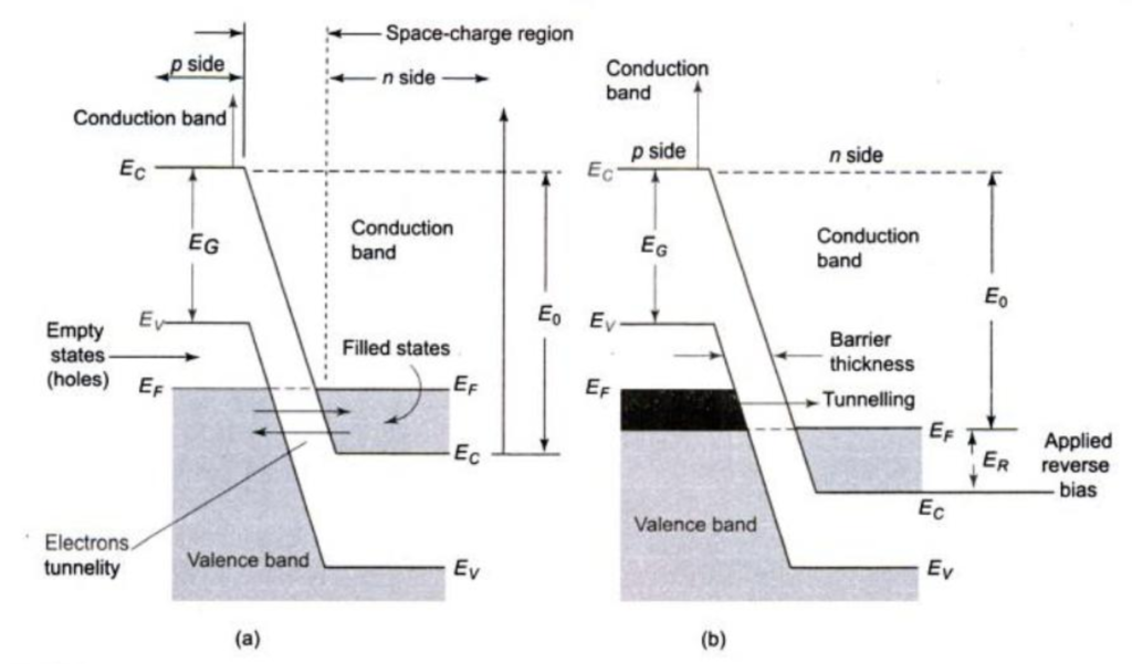
Tunnel diode operation when it is reverse biased
When the diode is reverse biased the energy gap between p and n-region increases. This difference will be more than energy gap. Now there are some energy states in the valence band of p-region which can be filled with the electron of n-region. Thus the electrons from p-region can tunnel through the depletion layer to reach and fill the spaces in the n-region. The number of electrons moving from p-region into n-region are more as compared to the electrons moving from n-region into p-region. This will result into the conventional current from n-region into p-region. As the reverse voltages are increased, the more electrons will tunnel from p-region into n region. This will result linear relation between the reverse voltages and the current as shown in the characteristics curves of Tunnel diode.
Tunnel diode operation when it is forward biased
When small forward biased voltages are applied then the energy gap will start decreasing as shown in the figure below. This difference will be less than
undefined
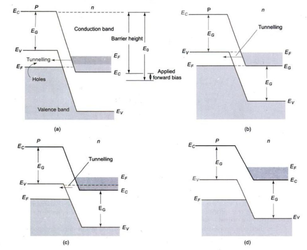
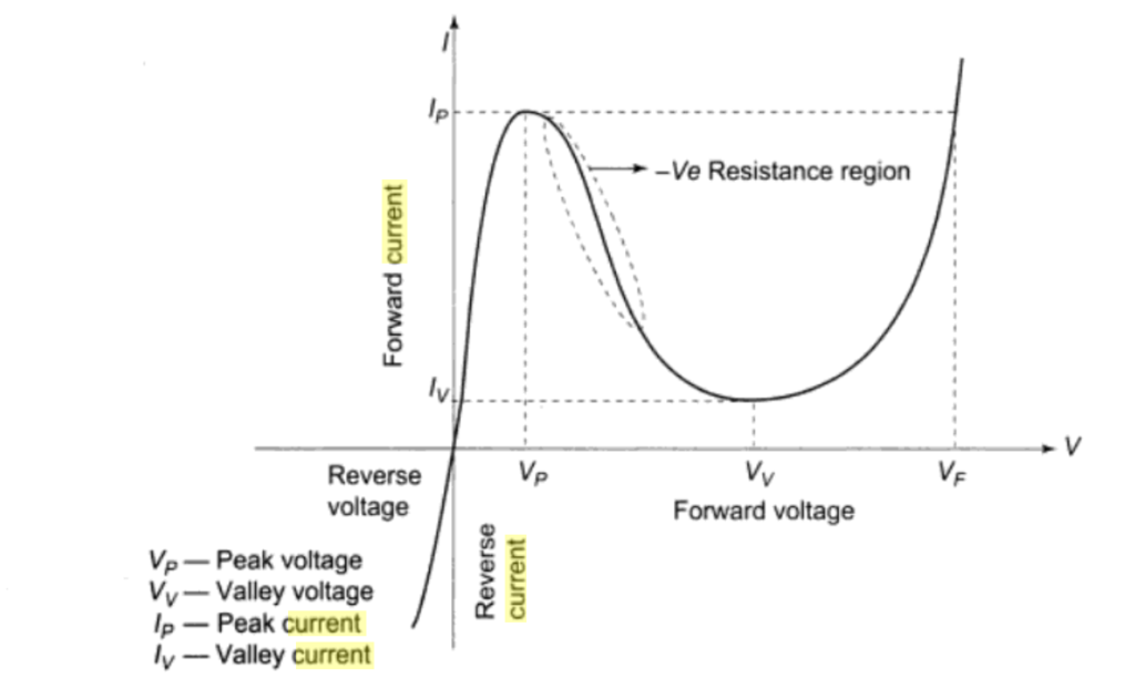
Now there are electrons in the conduction band of n-region which possess more energy than the electrons in the valence band of p-region. These electron will tunnel through from n-region into p-region causing large current flowing from n to p. The direction of the conventional current will be from p to n region. As the potential is increased, the more current will flow until a point is reached called the maximum current point. When the voltage is further increased, the electrons in the n-region will not tunnel into the p-region. Since there will exist the energy gap that will be more as compared to the energy states of valence band of p-region. Thus electrons with the higher energy in conduction band as compared to the valence band energy can not tunnel because of forbidden energy gap between these two regions as depicted in the above figure (d). Very few electrons will be able to tunnel through now. Hence with increase in voltage, current decreases thus showing the negative resistance phenomenon.
Equivalent circuit of Tunnel diode
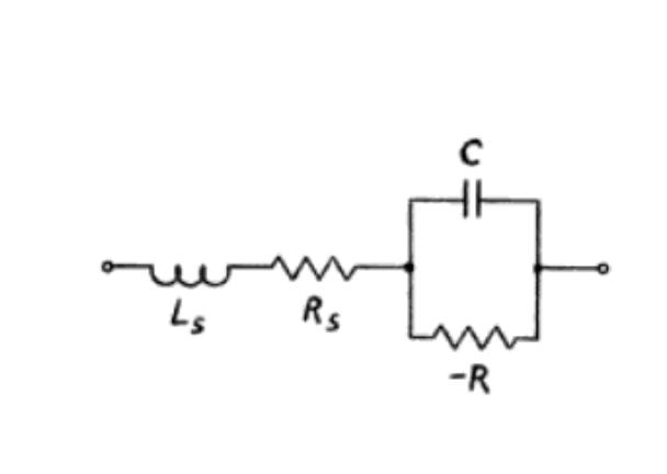
The diode works as a linear resistor when it is reverse biased and a negative resistor when it is forward biased. The voltages at which the maximum current flows when forward biased is called the peak voltages and the corresponding current is called the peak current. The voltages at which the minimum current flows is called the valley voltages and the corresponding current is called the valley current.
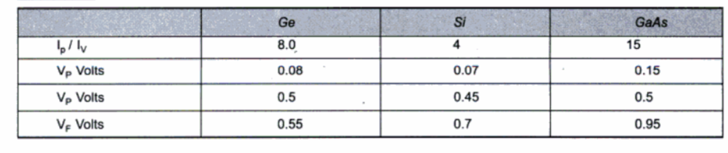
Typical properties of Tunnel diode
Typical properties of Tunnel diode are shown in the figure below
Applications of Tunnel diode
There are so many applications of Tunnel diode
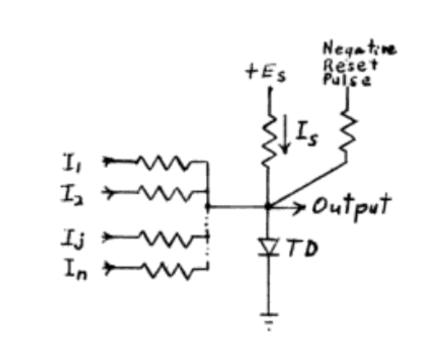
We can design a bistable Tunnel diode circuit that can be used either as an OR and an AND logic circuit as shown in the figure below
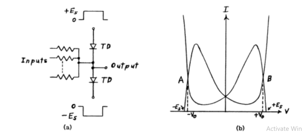
It can also be used for AC power locking operation as shown in the figure below
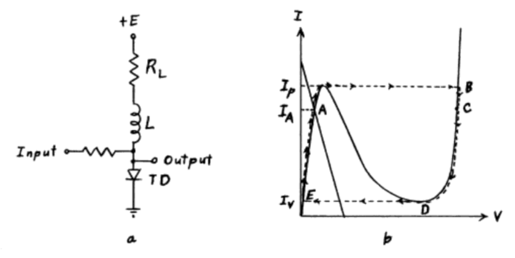
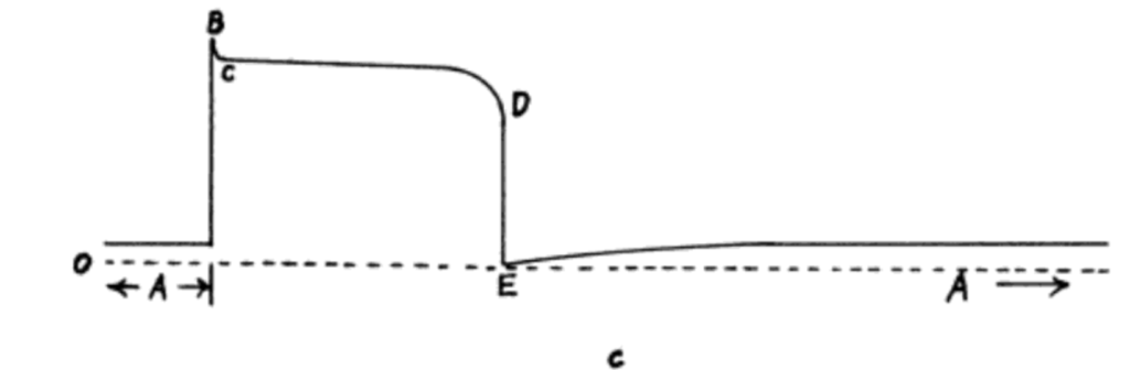
Also helpful for designing monostable oscillator. It can be noticed in the following figure that the static load line intersects the diode characteristics curve at only one point. If we apply small amount of current the circuit will switch to C point as shown below. Horizontal load line is obtained through the inductor. But the operation at C point can not be maintained still. So the current will decrease and the point of operation will be again at E thus producing pulse.
Also read here:
- What are the switching circuits of diode? Examples and Problems
- How to test a diode? When diode is working and when it is not working?
- How zener diode is used for voltage and line regulation?
- What is the varactor diode and how does it work?
- what is the difference between drift and diffusion current of a diode?
- What is the light emitting diode (LED)? How does it work?
- What is the barrier potential of PN junction diode ?
One thought on “How Tunnel diode works?”