What are the Diode Models?
In this article I have discussed in detail what is the diode ideal and practical model. How do we treat the diode as a circuit element? Which diode model is best while analyzing or designing a circuit. Basically diode is a pn junction device and we can analyze any circuit in three possible ways when that circuit contains a diode in it.
There are three models of the diode:
- Ideal model
- Practical model
- Complete diode model
What is the Ideal Diode Model?
This is the most simple approach where we treat the diode as an ideal element. By ideal we mean, we will ignore the barrier potential of the diode that is 0.7v in case of silicon and 0.3 v in case of germanium when it is forward biased. So, when diode is forward biased, we will say infinite amount of current is flowing with zero voltage drop across its terminals. When it is reverse biased, we will say it has infinite resistance and hence zero leakage current across its terminal.
The ideal diode model is not much accurate model and can be modeled as a simple switch.
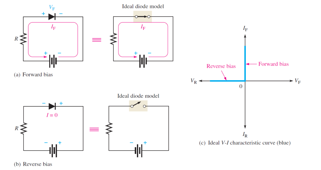
In this model we have ignored barrier potential, forward dynamic resistance and reverse leakage resistance. This model is helpful for troubleshooting or while checking diode is working or not properly. We get the following equations in this case
VF=0V
undefined
IR=0A
VR=VBIAS
What is the Practical Diode Model?
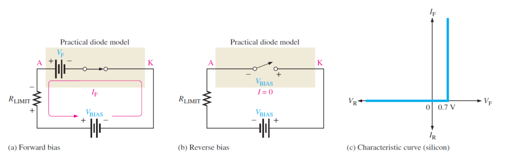
In this model barrier potential is included. When diode is forwarded biased it is considered as a closed switch with a voltage source connected in series. This voltage source is actually a barrier potential that must be exceeded by the external battery in order to cause the conduction. When diode is reverse biased it is equivalent to an open switch just like in case of ideal diode model. The barrier potential has no effect on reverse bias.
The calculations can be done using the following formulas
VF=0.7V
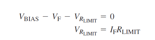
IR=0A
VR=VBIAS
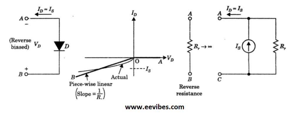
What is the Complete Diode Model?
As its name indicates, all the parameters that we neglected in ideal model are now considered. So when diode is forward biased, a voltage source of 0.7v and a small dynamic resistance connected in series is considered with external biased voltages. While in reverse bias condition it is again an open switch but with a large reverse resistance connected in parallel with a switch. This resistance provides path to the leakage current that is present always. This is the most accurate approximation of the diode as it considers all parameters of it during analysis.
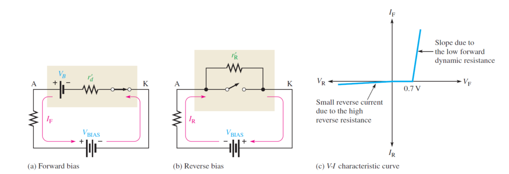
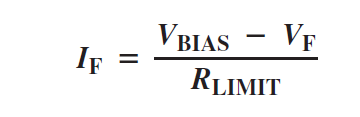
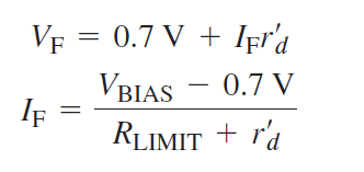
The graph for the complete diode model is appeared in Figure (c). Since the barrier potential and the forward dynamic resistance are included, the diode is expected to have a voltage across it when it is forward biased. This voltage (VF) comprises of barrier potential plus the small voltage drop across the dynamic resistance. The curve slops as the voltage drop across the dynamic resistance increases because of increase of current. For the complete model of a silicon diode, the equations we can apply are:
The reverse leakage current is shown on the left side of the graph. Since the breakdown operation is not a normal operation for most of the diodes that is why it is not shown in the characteristics curves.
Example of Practical Diode Model
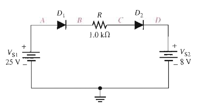
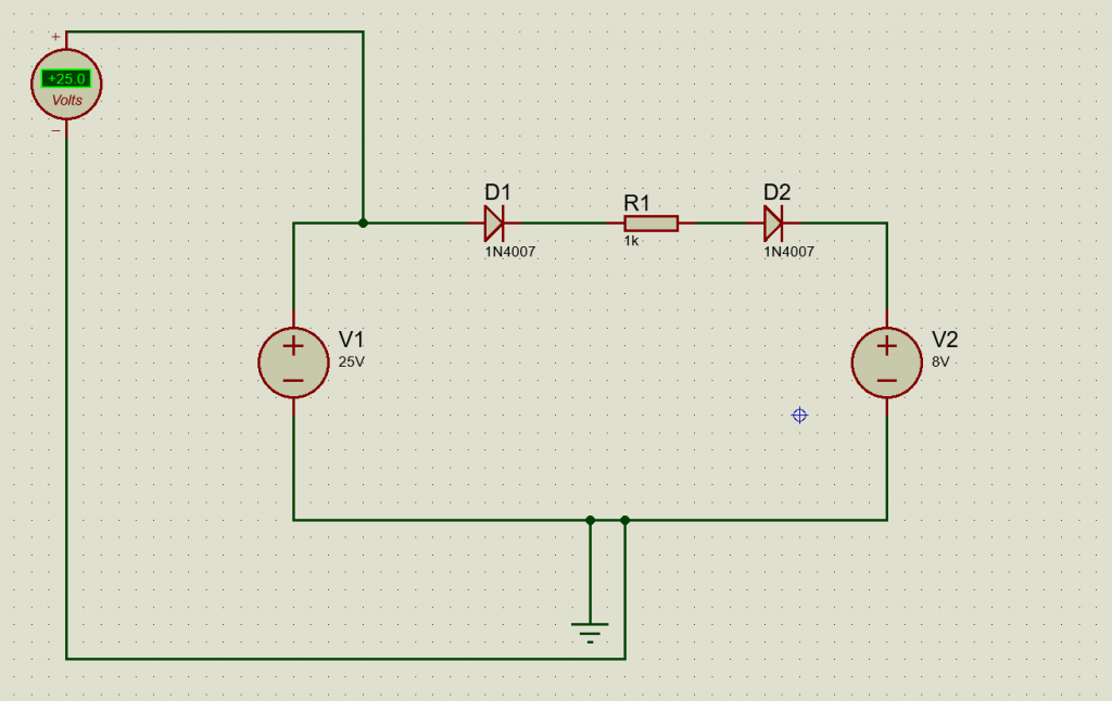
Find the voltages at each point with respect to ground in the following circuit using practical diode model.
Solution
As mentioned above in complete model we assume the forward voltage drops across the diode (VF=0.3V in case of Ge and 0.7V in case of Si)
Applying KVL, we get
-25+0.7+IFK+0.7+8=0
-17+1.4+ IFK=0
15.6=IFK
——à IF=15.6mA
This is the forward current flowing in the circuit
Now, let’s calculate the voltages at each point
At point A
VA=25V as at this point the battery or source is connected and there is no voltage drop.
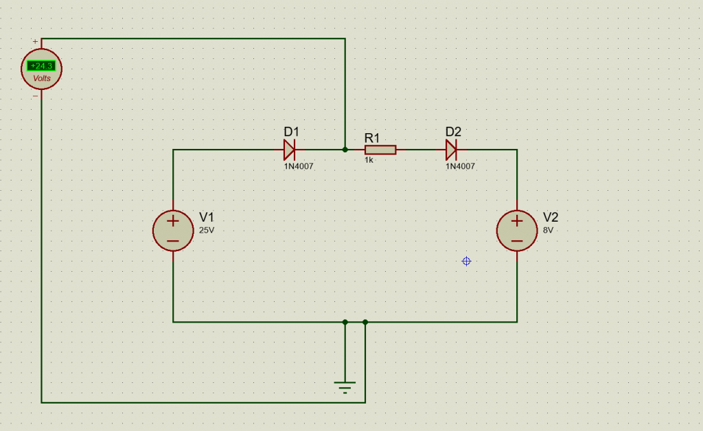
At point b
VB=25V-0.7V=24.3V
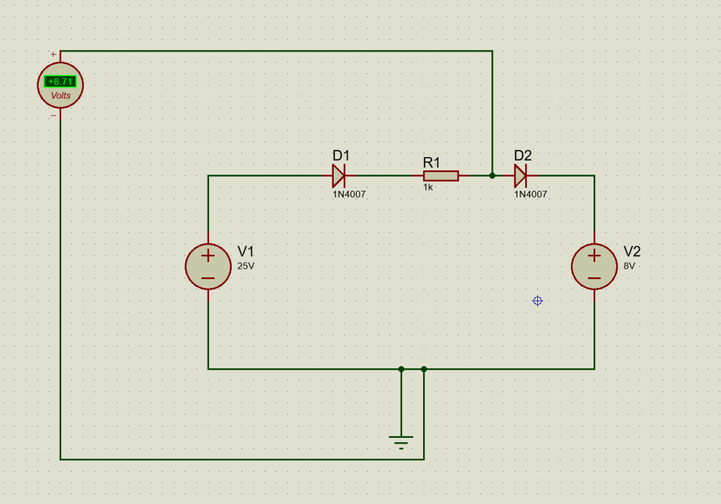
At point C
Voltage is equal to
25V-0.7V-(15.6mA)(1K)=25V-0.7V-15.6V=8.7V
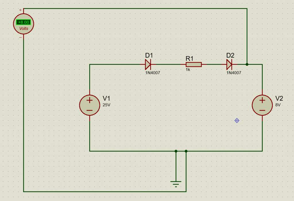
Now at the last point D
VD=8V as it is directly connected with 8V battery terminal
5. Determine whether each silicon diode in Figure 2–92 is forward-biased or reverse-biased.
6. Determine the voltage across each diode in Figure 2–92, assuming the practical model.
7. Determine the voltage across each diode in Figure 2–92, assuming an ideal diode.
8. Determine the voltage across each diode in Figure 2–92, using the complete diode model with rd=10Ω and rR=100M Ω
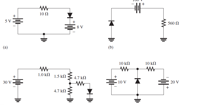
Solution:
Part 1;
part 2:
Which Diode Model is Better for a Circuit? Ideal, Practical or Complete?
If we are generally solving a numerical problem then it is preferable to use an ideal diode model where the voltages dropped across a diode are not of significance importance. For example when you are designing an inverter or a switch, it is better just to consider the 0 voltage drops when it is ON and V-bias voltages when it is OFF. While working in your college laboratory it is better to use a practical model of diode. Where you will consider 0.7V voltage drop across a diode. Complete diode model is used when you are analyzing a simple circuit or when a circuit is not much complex. Since it would be easier to consider the effect of dynamic resistance and reverse resistance for better understanding.
watch here for video lecture
Also read here:
- How Tunnel diode works?
- What are the switching circuits of diode? Examples and Problems
- How to test a diode? When diode is working and when it is not working?
- How zener diode is used for voltage and line regulation?
- What is the varactor diode and how does it work?
- what is the difference between drift and diffusion current of a diode?
- What is the light emitting diode (LED)? How does it work?
- What is the barrier potential of PN junction diode ?