What is a Full Adder Circuit?
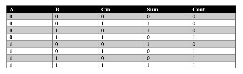
A full adder is a circuit that adds three inputs (A,B,Cin) where Cin is any carry in while performing addition of binary numbers and produces output Sum and Cout which is the carry out.
The truth table shows below how full adder circuit works.
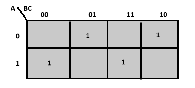
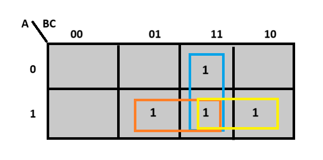
We can use the k-map for simplifying the final expressions of Sum and Cout.
The sum output of a full adder is given by:
\[
S = A \oplus B \oplus C_{in}
\]
Alternatively, in terms of AND, OR, and NOT gates:
\[
S = (A \oplus B) \oplus C_{in} = (A \overline{B} + \overline{A} B) \overline{C_{in}} + \overline{(A \overline{B} + \overline{A} B)} C_{in}
\]
k-map for Cout is:
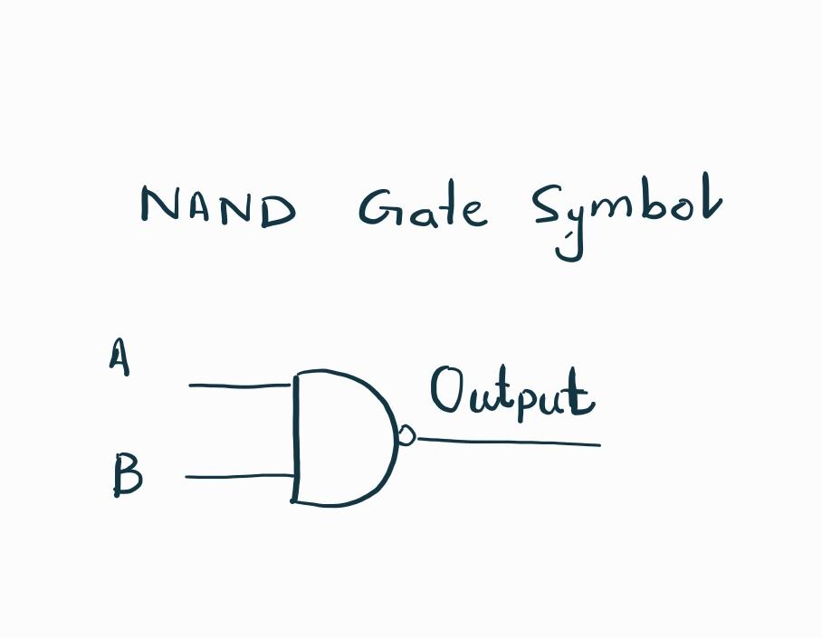
What is the NAND Gate?
A NAND gate is the logical gate that takes the two or more inputs and produces the NOT of AND of those inputs. NAND gate is also known as the universal gate as we can implement any logical expression using it. The NAND gate is the combination of two logic gates NotAND.
The NAND gate combines the actions of an AND gate followed by a NOT gate. It is one of the most important gates in digital electronics because it is functionally complete, meaning that any logic function—such as NOT, AND, OR, or even more complex circuits—can be constructed using only NAND gates. This property makes it highly valuable in the design of integrated circuits and digital systems.
Symbol and Logical Expression of NAND Gate
Here is the logical expression along with its symbol. Also, the truth table can be seen for understanding the concept of NAND operation.
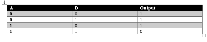
Output= (A.B)’
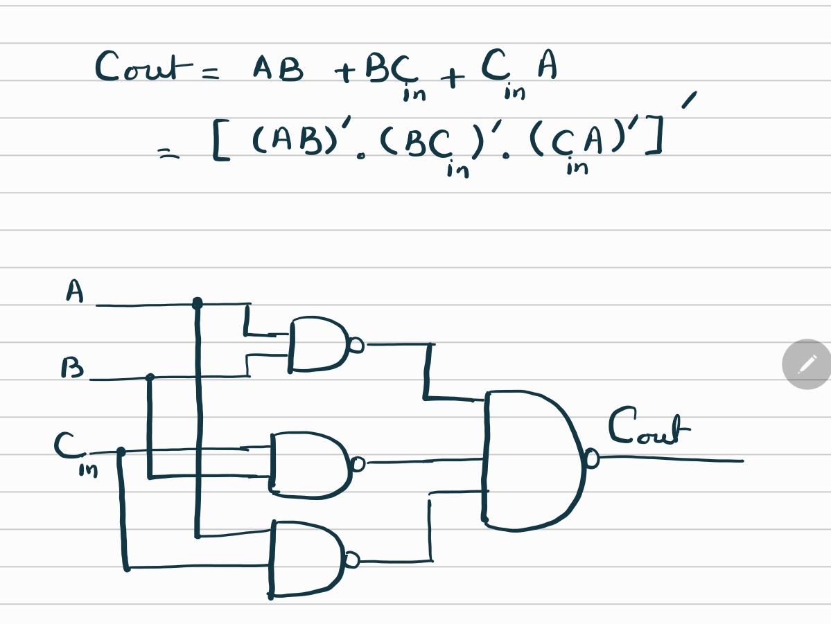
Implementation of Cout Function of Full Adder using NAND Gates Only
The carry output $C_{out}$ of a full adder is given by:
\[
C_{out} = AB + BC_{in} + AC_{in}
\]
Using DeMorgan’s theorem, it can be written using complements (bar notation) as:
\[
\begin{aligned}
C_{out}
&= \overline{\,\overline{AB + BC_{in} + AC_{in}}\,} \\
&= \overline{\,\overline{AB} \cdot \overline{BC_{in}} \cdot \overline{AC_{in}}\,}
\end{aligned}
\]
where
\[
\overline{AB} = \overline{A \cdot B}, \quad
\overline{BC_{in}} = \overline{B \cdot C_{in}}, \quad
\overline{AC_{in}} = \overline{A \cdot C_{in}}
\]
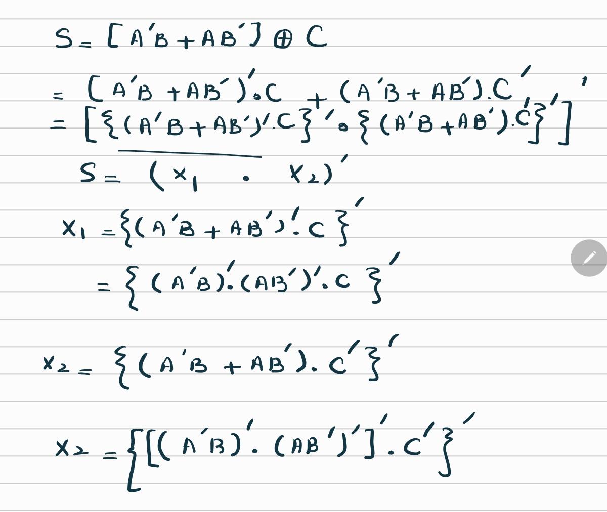
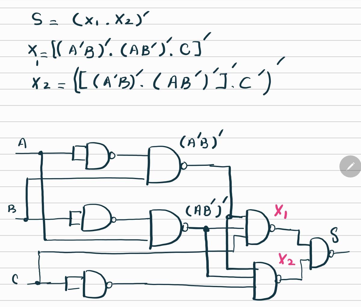
Implementation of Sum Function of Full Adder using NAND Gates Only
The sum output S of a full adder using complement (bar) notation is given by:
\[
\begin{aligned}
S &= (A \oplus B) \oplus C_{in} \\
&= (\overline{A} B + A \overline{B}) \overline{C_{in}}
+ \overline{(\overline{A} B + A \overline{B})} C_{in}
\end{aligned}
\]
Using DeMorgan’s theorem, we get:
\[
\overline{(\overline{A} B + A \overline{B})}
= (\overline{\overline{A} \cdot B}) (\overline{A \cdot \overline{B}})
= (A + \overline{B})(\overline{A} + B)
\]
So finally:
\[
S = (\overline{A} B + A \overline{B}) \overline{C_{in}}
+ (A + \overline{B})(\overline{A} + B) C_{in}
\]
Circuit Diagram of Full Adder Circuit Using NAND Gates Only
Applications of Full Adders in Engineering
The full adder is a fundamental building block in digital electronics, widely used in various engineering applications where binary addition is required. One of its primary uses is in the design of arithmetic logic units (ALUs) within microprocessors, where full adders perform binary addition of multi-bit numbers by cascading multiple full adders to form ripple-carry adders.
Full adders are also essential in the implementation of multipliers, where partial products are summed up using arrays of adders. In digital signal processing (DSP), full adders are integral to operations such as convolution and filtering that rely on high-speed arithmetic.
Additionally, they are employed in counters, checksum generators, and digital comparators, enabling reliable computation and data integrity checks. Beyond these, full adders are used in hardware systems requiring binary-coded decimal (BCD) arithmetic, such as digital clocks and calculators, and serve as core components in custom VLSI designs, making them indispensable across computer engineering, embedded systems, and communication hardware.