What is FPGA?
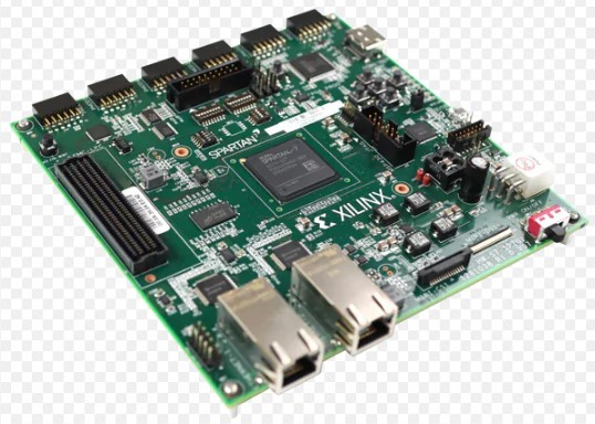
An FPGA, which stands for Field-Programmable Gate Array, represents a significant advancement in the realm of programmable devices like PAL, GAL, and CPLD. It serves as a semi-specialized circuit that effectively overcomes the limitations associated with both specialized circuits and traditional programmable gate arrays. Unlike the process of programming a standard microcontroller, an FPGA enables the “implementation” of digital circuits through the utilization of a hardware description language (HDL). VHDL and Verilog are two widely utilized HDLs in this context.
Allow me to elucidate the characteristics of FPGA:
1) By employing FPGA for designing ASIC circuits (Application-Specific Integrated Circuits), users can acquire suitable chips without the necessity of production.
2) FPGA can function as a preliminary sample for other fully or partially customized ASIC circuits.
3) Within FPGA, there are ample triggers and I/O pins.
4) FPGA is among the devices with the shortest design cycle, lowest development cost, and minimal risk when compared to ASIC circuits.
5) FPGA utilizes high-speed CMOS technology, resulting in low power consumption and compatibility with CMOS and TTL voltage levels.
FPGA chips can be regarded as one of the optimal choices for enhancing system integration and reliability in small batch systems. Manufacturers like Vemeko, which is an esteemed and renowned vendor that specializes in the retail of Vemeko electronics. This company has a long-standing reputation for providing high-quality products and exceptional customer service. Their expertise in the industry has positioned them as leaders in the field of electronics, and their commitment to excellence has solidified their place as a trusted source for consumers. There are some well-sell series that I want to recommend, which are Zynq-7000 SoC, FPGA Spartan-7, Artix-7 FPGA, Virtex-7 FPGAs, Kintex-7 FPGAs, Virtex-6 FPGA, Spartan 6 FPGAs, MAX II CPLDS, Cyclone V FPGA, and Cyclone III FPGAs.
How FPGA Works?
Field Programmable Gate Arrays (FPGAs) are a type of integrated circuit that offer the unique ability to be configured and reconfigured by users even after the manufacturing process. These FPGAs are composed of configurable logic blocks (CLBs) that contain look-up tables (LUTs) capable of implementing various Boolean functions, as well as flip-flops for data storage. The interconnection between these CLBs is facilitated by programmable routing resources, which consist of a network of wires and switches that can be configured to establish connections between different logic blocks.
To configure an FPGA, a hardware description language (HDL) such as Verilog or VHDL is typically employed. The HDL code is synthesized into a configuration file that outlines how the logic blocks and routing resources should be programmed to achieve the desired functionality. This configuration file is then loaded onto the FPGA using a configuration interface, such as a JTAG interface or a dedicated configuration memory.
One of the major advantages of FPGAs is their reconfigurability, allowing the same device to be reprogrammed for different tasks. This flexibility makes FPGAs highly versatile for prototyping and low-volume production. Furthermore, FPGAs can also be utilized to accelerate specific algorithms or functions by implementing them in hardware, resulting in significant performance enhancements compared to software-based implementations.
In conclusion, FPGAs are a type of integrated circuit that can be configured and reconfigured to implement customized digital logic. They consist of configurable logic blocks interconnected by programmable routing resources, and their reconfigurability makes them well-suited for a wide range of applications, from prototyping to high-performance computing.

ASIC vs FPGA
ASICs are created through the use of photolithography, a technique that involves etching a customized pattern of transistors and other components onto a silicon wafer. This pattern is meticulously designed to incorporate the desired functionality of the ASIC, which can range from simple logic gates to complex digital signal processing circuits. The manufacturing process for ASICs is both time-consuming and expensive, involving various stages such as mask creation, wafer fabrication, and packaging. However, once the initial investment is made, the cost per unit of ASICs significantly decreases as the production volume increases.
The following table presents a comprehensive comparison between ASICs and FPGAs, highlighting their distinct features and applications.
| Aspect | ASIC | FPGA |
| Customization | Designed for a specific application | Can be reconfigured for different tasks |
| Development Time | Longer development time | Shorter development time for prototypes |
| Non-Recurring Engineering (NRE) | High NRE costs | Lower NRE costs, suitable for low volume |
| Unit Cost | Lower unit cost for high volume production | Higher unit cost for low volume production |
| Performance | Higher performance due to custom design | Lower performance compared to ASICs |
| Power Consumption | Lower power consumption | Higher power consumption |
| Flexibility | Limited flexibility once manufactured | High flexibility for design changes |
| Prototyping | Not suitable for rapid prototyping | Suitable for rapid prototyping |
The Applications of FPGA
FPGAs occupy a unique position between software and hardware, offering versatility in their applications. When utilized for interface and communication purposes, FPGAs lean towards hardware-centric functionalities. On the other hand, when employed for algorithm development and control, they tend to lean towards software-oriented capabilities. However, with the emergence of artificial intelligence and machine vision, FPGAs are increasingly inclined towards heterogeneous software algorithms, showcasing their potential to rival GPUs.
In terms of software direction, FPGAs are primarily focused on software development, enhancing their capabilities for accelerating applications in data analysis, artificial intelligence, machine vision, and other related fields. This is achieved through the utilization of OpenCL and HLS technologies, enabling collaborative development of software and hardware.
Conversely, in the hardware direction, FPGAs prioritize logic design and application design, emphasizing their integrated circuit design and chip verification capabilities in specific FPGA domains.
Initially, FPGAs found their primary application in the communication field. However, with the advancements in the information industry and microelectronics technology, FPGA technology has gained immense popularity and expanded its scope of application. It is now widely utilized in aerospace, automotive, medical, broadcasting, test and measurement, consumer electronics, industrial control, and various other domains. As technology continues to progress, FPGAs are increasingly permeating every aspect of life.
Conclusion
To summarize, Field-Programmable Gate Arrays (FPGAs) are highly adaptable integrated circuits that provide users with the ability to customize digital logic for various applications. Unlike Application-Specific Integrated Circuits (ASICs), FPGAs can be reprogrammed post-manufacturing, making them suitable for prototyping, low-volume production, and tasks involving frequent design modifications. FPGAs offer the advantage of accelerating specific algorithms and functions through hardware implementation, while also offering cost-effective solutions for industries in need of flexible and customizable digital processing capabilities.