Table of Contents
Problem statement
In this post, you will learn about the design of an Arithmetic Logic Unit (ALU) with Hybrid Memristor CMOS Architecture which is actually an advanced 1-bit ALU. This work described is based on the architecture of ALU has focused on the following given areas:
- Improve signal degradation by lessening it in each and every stage and hence in the overall ALU circuit
- Decreasing the transistor count by replacing it with memristors of less
- The designing and simulation of the basic oriented building blocks of ALU with the help of a hybrid combination of CMOS-memristor
- This model compares with current state-of-art ALU models based on transistor-memristor approached hybrid ALU structure.
INTRODUCTION:
A memristor is a two terminal non-linear component that helps in the relativity of magnetic flux with the electric flux. It works like a resistor whose resistance is dependent on the previous flowed charge through the device.
In processors, one of the major building blocks is ALU. Due to the limitations of ALU, complex computer processors require a lot of time and area. So, memristors are considered as a good candidate for modeling ALU due to its smaller area and delay. However, when multiple Memristor Ratioed Logic (MRL) gates are cascaded, it will degrade the output signal substantially. When the input voltages are distinct, MRL gates get to suffer from the sneak path (undesired path) of current flow resulting in high power static consumption. This proposed ALU model by integrating memristor CMOS logic circuits brings much improvement in the work.
The proposed 1-bit ALU model having nine functionalities, And it is fully cascadable. 1-bit ALU is implemented by integrating Memristor Ratioed Logic (MRL) gates and CMOS elements (180nm). The behavioral analysis is done using LTSpice. LTSpice (an analogue electric component simulator software) is used for simulation of the proposed mechanism of 1 bit ALU. This helped in changing the parameters according to the model of the components used. With the simulation, an optimizable cascaded 1 bit ALU with the binary logic states based on voltage level is designed and analyzed.
Before starting how to design an arithmetic logic unit lets first see what are the memristors?
What are the Memristors?
A memristor is a two terminal non-linear component that helps to relate magnetic flux with the electric flux. It is one of the most elemental electric component which is based on the working of a non-volatile memory component which means that it can retain its pass by state through its resistive property.
CMOS:
CMOS means a Complementary Metal-Oxide Semiconductor. It is basically a transistor which uses p-type and n-type MOSFETs for the implementation of logic functions. The construction of integrated circuit uses the CMOS Technology in order to design an arithmetic logic unit.
Multiplexers:
A multiplexer (MUX) is a device that can receive multiple input signals and combine these signals to form a single output signal in a retrievable manner for each input signal.
METHODOLOGY:
The V-I characteristic of memristive devices is basically a hysteresis loop. This V-I property helps memristor to retain its previous state and is dependent on the previously applied voltage.
Memristor is based on this equation of associating the magnetic flux and electric flux
dφ = M. dq
Like other resistive elements, memristor is also a two-terminal component. But memristor has polarity factor which makes it different from resistance. The black line in its symbol identifies the polarity of a memristor. Its resistance depends on the path of current flow. When the current flows into the device, its resistance decreases and when out of the device, its resistance increases. The threshold voltage here is ±0.2V . Within this range of input voltage, the memristor shows minimal resistance, and this state is considered ON state of the memristor. Outside this range the memristor shows very high resistance, and this state is considered OFF state for the memristor.
A primary 1-bit Arithmetic Logic Unit typically have two inputs which gives one output which is dependent on the selection bits. The Arithmetic Logic Unit structure performs various arithmetic operations, conditional and logical operations. These operations are performed by implementing some building blocks in ALU structure like, multiplexers and logic blocks. Memristor Ratioed Logic used to form OR and AND gates and here threshold voltage logic is used instead of memristance based logic. Two binary inputs are taken by the gates taking into consideration that the high voltage is represented by ‘1’ and low voltage is stated as a logic ‘0’. The output shows the voltage logic state which is in this case 1.8V for logic 1 and 0V for logic
- For construction of larger logic circuits, it would be counter-instinctive if we just use AND and OR gates because they only give positive logic. As, inversion is also fundamental for complex logic operations. The combination hybrid model uses CMOS (180nm) for logic inversion. Hybrid Memristor-CMOS gates are high area efficient as comparable to the pure CMOS gates. Design of arithmetic logic unit.
Memristor works like a resistor in every of its state. If a bigger circuit is constructed using pure memristor, then consequential signal degradation is noted. That’s why, when MRL gates are cascaded directly then it will show highly degraded output. Therefore, this structure is adjusted to lessen the signal loss and hence used as a basic building block of ALU. To refrain the direct connection of the gates of memristor, two inverters are introduced in the block. Hence, when the various blocks are cascaded, the output signal will remain constant. Design of arithmetic logic unit.
This altered block is known as ‘NAND-NOR-XOR’ block. The modified block contains two binary inputs and gives three distinct logic outputs i.e., NAND, NOR and XOR. The inputs are first processed concurrently by the memristive OR and AND gates. The input and output voltage levels are 1.8V, which is equivalent to the voltage supply of the CMOS inverter. The ALU structure use outputs from CMOS circuits just to ensure the stability and consistency of working throughout the circuit. The arithmetic logic unit gives just one output which is dependent on the selection bits. This needs the working of a multiplexer. For the reduction of signal degradation, a modified 2-to-1 multiplexer(MUX) is used which is then cascaded to construct a 4-to-1 MUX.
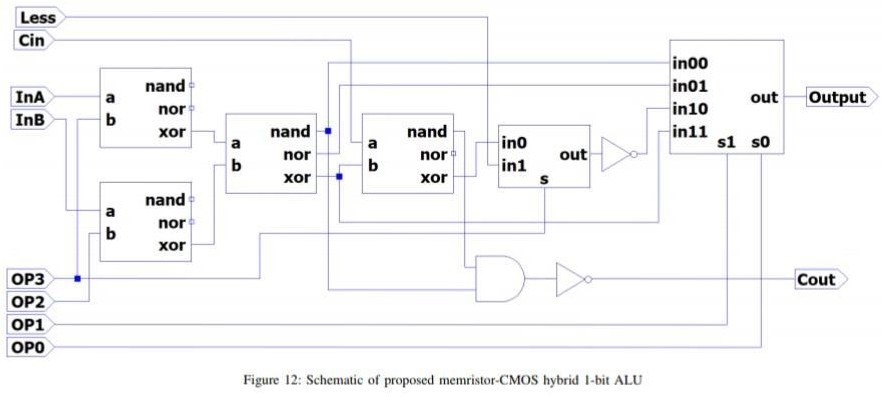
The 2-to-1 multiplexer is produced by the combination of the outputs of AND gate MRL and an OR gate MRL with a CMOS inverter. In ALU, for signal propagation, the output of the inverter is used. As a result, Inversion of the input signal is the output of the block. For construction of bigger multiplexer, the output of a modified 2-to-1 MUX is inverted and can used as a building block. To effectually refrain from the signal loss inside the circuit and the substitution of function of a buffer with reduced logic elements, we use the inverter at the output. The hybrid structure is constructed from the MRL gates. And a stable current flowing through the MRL gates between the two inputs causes a high static power consuming for use in the opposite input signals. As follows,
P static=V2high/RON+ROFF
The equation gives a lower static power consumption as compared to previous proposed works.The CMOS-memristor structure block uses inverters with a supply of power(1.8V). This proves to be right for the CMOS(180nm) to help keep the output signal constant throughout the Arithmetic Logic Unit circuit. This proves to be significant for the connection of the components in a huge circuit which gives an output signal in the absence of significant degradation and failure. These building blocks are afterwards connected for the construction of 1-bit Arithmetic Logic Unit (ALU) architecture.
The architecture of proposed ALU consists of four ‘nand-nor-xor’ blocks, one MRL AND gate, two CMOS inverters, one 2-to-1 multiplexer and one 4-to-1 multiplexer. To performing addition the 1-bit ALU implements a full adder, by taking two inputs and Cin. ALU is
expanding to higher bit sizes when Cin and Cout bits enables. Subtraction operation is done by using 2’s compliment method. For SUB operation the Cin bit is set as ‘1’ .
RESULTS:
The proposed hybrid mesmristor-CMOS ALU focused on following results:
- The Proposed memristor-CMOS uses much less number of transistors by replacing them with MRL logic gates and instead of using whole buffer they use Hence, the proposed 1-bit ALU has much smaller area than conventional ALUs.
Note:
In this work the size of the memristor model used is approximately 3nm with area approximately 9nm2.
- In previous works, severe signal loss (∼15%) shows while directly cascading multiple MRL This work makes output signal degradation nominal (∼4.65%) reduces this loss to minimum extend.
- The worst scenario of propagation delay occurs for ‘SUM’ operation with in the proposed ALU. When this propagation delay is compared, it shows 92.83% improvement over standard 180nm CMOS ALU in the proposed hybrid
CONCLUSION:
In 1971, L. Chua invented memristor but it did not get much attention until the recent years. When HP implemented the usage of memristor then it got quite attention. Because of its small size, it is low power consuming and have high switching capability. So, that’s why researchers focused on its possibilities and considered it to be used in logic circuitry, artificial neural network and in non-volatile memory devices.
The first hybrid memristor-CMOS logic block is proposed by Mehri Teimoori et al. The complete ALU structure model can be implemented by using the Hybrid CMOS-memristor structure, which has been the focus of several recent works. The working of MRL gates are not suitable to implement ALUs on its own as the operation of MRL gates is based on voltage oriented logic variable which works by using the positive logic scheme.
The architecture of hybrid model of ALU, focuses on these parameters e.g., functionality, modularity, transistor count minimization, signal loss reduction and delay improvement. Using 180nm CMOS transistor along with voltage threshold based MRL gates in this work and to verify the proposed models and the ALU it is simulated in LTSpice. Our proposed ALU is much smaller in area than purely CMOS architecture ALU is done by the decreasing transistor count. CMOS-MRL hybrid architecture is a improved version of previous ALU models with more operational functions. Due to the modified architecture the signal degrades by only 4.65%.
FUTURE WORK:
This proposed architecture of hybrid model of ALU, focuses on functionality, modularity, transistor count minimization, signal loss reduction and delay improvement. Whereas, work on the total power consumption and switching characteristics of the proposed model will have scope in future. This work hopes to pave the path for designing more complex computational models by using hybrid memristive circuits. Furthermore, many researches have also been done on model of hybrid memristor CMOS based full adder and it’s energy was evaluated for each additional operation.
Also read here
https://eevibes.com/digital-logic-design/how-to-represent-the-boolean-function-in-canonical-form/
what is the Canonical form representation of Boolean function?