Introduction
In PCB design, a library is also a file or a database for organizing elements that can be re-used many times during physical design. PCB libraries include symbol libraries that hold schematic design symbols; footprint libraries that contain device footprints (land patterns), and model libraries with models for the simulation programs.
While these three aspects of a library element are combined in a single technology library in IC chip design, they are typically stored in separate (technology) libraries in PCB design.
The libraries can typically be searched with a library management system. When the PCB design is being drawn, copies of the required elements are placed in the circuit schematic or layout. Here too, this procedure is referred to as instantiation, as with chip design.
Within the PCB library, different library elements can reference one another. PCB libraries are often tied to specific tools and tool providers; as a result, symbol, footprint and model libraries for PCB design are often not interchangeable between different design tools. These libraries are stored in either ASCII or binary formats, depending on the tool provider.
What Are PCB Design Libraries?
A PCB design library is a collection of electronic component definitions used by PCB design software. These definitions help represent components in circuit diagrams and determine how they will be placed and connected on a physical circuit board.
A typical library component may include a schematic symbol, a PCB footprint, pin numbers, electrical properties, dimensions, and a 3D model. The exact information depends on the software and the component library.
For example, when designing a PCB using a microcontroller such as the ATmega328P, an engineer may select its schematic symbol from a library and associate it with the correct physical footprint. The footprint specifies the locations and sizes of the pads where the component will be soldered.
Using the correct library part is important because an incorrect footprint or pin mapping can cause manufacturing defects or prevent the circuit from functioning correctly.
Types of PCB Design Libraries
PCB libraries contain several types of information that work together during the design process.
1. Schematic Symbol Libraries
Symbol libraries contain the symbols needed to create the circuit diagram shown below. They can be searched, viewed, selected and instantiated in the library management system. The symbol in a symbol library typically references to one or more suit- able footprints for the associated physical device. Other information, such as the manufacturer, the vendor or the link to electrical models can generally be stored as well.
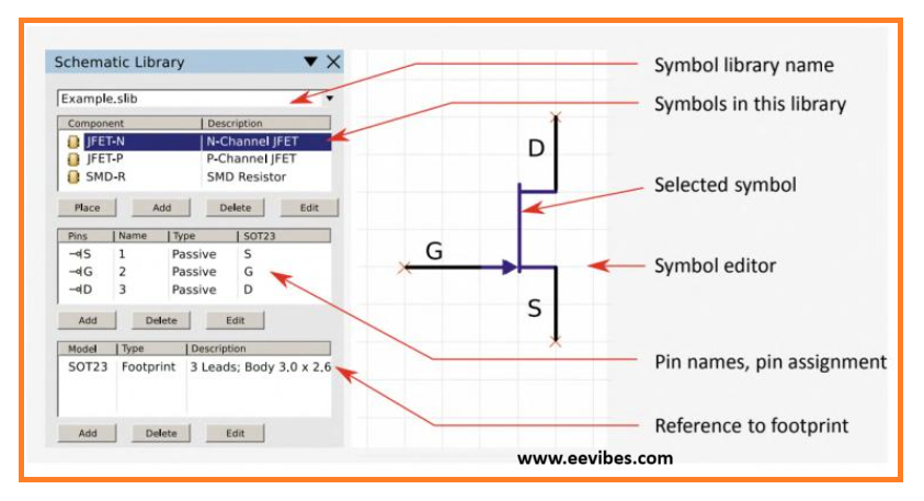
If the libraries being used do not contain a required symbol, design tools generally allow the designer to create a new symbol with a symbol editor and to store it in the symbol library. The new symbol should have all the necessary information for the design process, such as the link to the footprint, the pin assignment and, if necessary, the link to the electrical model.
2. Footprint Libraries
While the term “footprint” (also known as “land pattern”) is often used to describe the arrangement of pads or through-holes used to physically attach and electrically connect a component to a PCB, it is also applied in the context of libraries. Here, the term is used more broadly and encompasses all physical information for a device required for PCB design. Aside from the geometrical description of the individual layers (routing layers, solder-resist layer, solder-paste layer, silk screen layer, mechanical layer, drill holes, cut-outs, etc.), the footprint may contain three-dimensional (3D) physical device models, as well.
Footprints are managed in footprint libraries, an example of which is depicted in Fig. below.
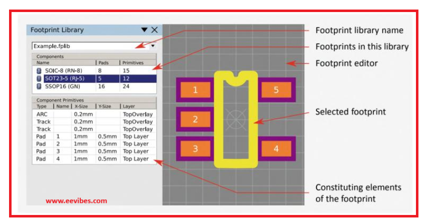
Every device symbol on the schematic refers to one (or more) associated foot- print(s) in the footprint library. This relationship is used during the transition from the circuit diagram to the PCB layout design to derive the associated footprints from the footprint library, which are then available for placement on the PCB.
New footprints can be designed in the footprint editor and stored in a library; however, care should be taken that the footprint is suitable for the prospective fabrication technology. If the PCB is needed as a 3D model in other fabrication steps, the matching 3D physical model must be included for the device.
3. Model Libraries
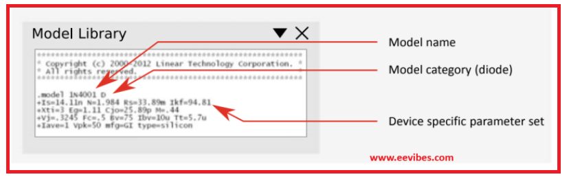
Electrical models for simulation programs, such as PSpiceTM, LTSpiceTM or SIMetrixTM, are arranged and stored in model libraries. They contain the written description of the device’s electrical response as shown in the following figure.
The model describes the electrical behavior of basic elements, such as resistors, capacitors, and inductances. Models of semiconductor diodes and transistors are adapted to the device in question by means of a number of characteristic parameters. More complex devices are modeled by connecting a number of basic elements.
In order to protect their intellectual property, some vendor models are only avail- able as encrypted entities, which do not allow any insight into the inner workings of the simulation models.
4. 3D Model Libraries
Three-dimensional component models allow designers to visualise how components will appear on the assembled PCB. They are particularly useful for checking component height, connector placement, mechanical clearances, and enclosure compatibility.
Many PCB design tools support 3D models in formats such as STEP, although supported formats vary between applications.
4. Manufacturer-Specific Libraries
Some manufacturers provide component libraries for their own products. These libraries may include verified symbols, footprints, pin mappings, and 3D models.
Manufacturer-specific resources can be especially useful when working with integrated circuits, connectors, power modules, and other components with detailed package requirements. Nevertheless, designers should always compare library data with the latest official datasheet.
Best Libraries and Resources for PCB Design
Several PCB design platforms provide built-in libraries, while independent websites offer downloadable symbols and footprints. The best choice depends on your software, project requirements, and experience level.
1. KiCad Libraries
KiCad is a popular open-source PCB design application used by students, hobbyists, researchers, and professional engineers. It provides schematic capture, PCB layout, design-rule checking, and 3D visualisation.
Its official libraries contain a large collection of schematic symbols and PCB footprints. Users can also create custom library components and maintain project-specific libraries.
KiCad is particularly suitable for students and engineers who want a powerful PCB design environment without paying for a commercial software licence.
2. Autodesk EAGLE Libraries
Autodesk EAGLE has historically been widely used for schematic design and PCB layout, particularly in hobby electronics and embedded systems. Its library ecosystem includes component symbols, packages, and device definitions.
However, Autodesk has discontinued EAGLE as a standalone product, with its final support ending in 2026. Users starting new projects should check Autodesk’s current Fusion Electronics offerings and compatibility requirements rather than relying on older EAGLE tutorials alone.
EasyEDA Libraries
EasyEDA is a browser-based electronics design platform that offers schematic capture and PCB layout. It is useful for beginners because users can work online and access a large collection of community and manufacturer-associated component information.
Its library resources can help designers locate symbols and footprints for common components, connectors, development boards, and integrated circuits.
Before using a community-submitted component, verify its dimensions, pin mapping, and electrical properties. A component appearing in the library does not automatically mean its data has been independently validated.
SnapEDA
SnapEDA is a component library resource that helps engineers find schematic symbols, PCB footprints, and 3D models for electronic components. It supports workflows involving several popular PCB design applications.
It can be particularly useful when a required component is missing from the default library supplied with the design software. Users should check the available download formats and verify the selected component against its manufacturer’s datasheet.
Ultra Librarian
Ultra Librarian provides downloadable electronic component models and library data for PCB design. Depending on component availability, resources may include schematic symbols, PCB footprints, and 3D models in formats compatible with different design tools.
It is useful for engineers who work with specific integrated circuits or need component models for established design workflows.
SamacSys Component Libraries
SamacSys provides electronic component library resources and CAD-model tools for supported PCB design applications. Its component models may include schematic symbols, footprints, and 3D representations.
These resources can save time when adding specialised components to a schematic or PCB layout. As with other third-party libraries, designers should verify model compatibility and physical dimensions before fabrication.
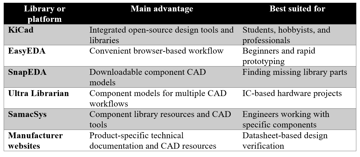
Comparison of Popular PCB Library Resources
How to Choose the Right PCB Library
Choosing a PCB library requires more than finding a component with the correct name. A reliable library part must match the exact device and package used in the project.
First, identify the complete manufacturer part number. Components with similar names may have different pinouts, package sizes, or electrical characteristics.
Second, confirm that the footprint matches the datasheet. Check pad dimensions, pin spacing, package outline, thermal pads, and pin-one orientation.
Third, verify the mapping between the schematic symbol and footprint. Each electrical pin must correspond to the correct physical pad.
Fourth, check whether the library includes the 3D model if mechanical verification is required. This is particularly important for connectors, tall components, and boards installed inside enclosures.
Finally, review the library’s source and version. Official or well-maintained libraries are generally preferable to unverified downloads, but every component should still be checked before manufacturing.
How to Add a PCB Library Component
The exact procedure depends on the PCB design software, but the general workflow is similar across most applications.
- Open the schematic editor. Start a new project or open an existing circuit.
- Search for the component. Look for the component name, manufacturer part number, or device family.
- Select the schematic symbol. Confirm that the number and functions of the pins are appropriate.
- Assign the PCB footprint. Choose the package that matches the physical component you intend to purchase.
- Check the pin mapping. Ensure the schematic pins are connected to the correct footprint pads.
- Transfer the design to the PCB editor. Arrange the components and route the electrical connections.
- Run design-rule checks. Correct clearance, connectivity, and other detected errors.
- Inspect the layout in 2D and 3D. Check board dimensions, connector orientation, and component spacing.
- Generate manufacturing files. Export the required Gerber files, drill files, and assembly documentation for your manufacturer.
A design-rule check cannot identify every incorrect library definition. Manual verification against datasheets remains necessary.
Creating Custom PCB Libraries
Sometimes a component is too new, too specialized, or unavailable in the existing library. In these cases, engineers can create a custom symbol and footprint.
Start by obtaining the manufacturer’s datasheet and mechanical drawings. Create the schematic symbol with the correct pin numbers and electrical functions. Then build the footprint using the recommended pad sizes, spacing, and package dimensions.
If the component requires a custom 3D model, add it using a format supported by the design application. Give the symbol, footprint, and model clear names, and store them in a project or shared library with appropriate version control.
Before using the custom component in a production design, check its pin-to-pad mapping, dimensions, orientation, and soldering requirements. For difficult packages, a prototype PCB can help confirm that the footprint works as intended.
Common PCB Library Mistakes to Avoid
Incorrect library data can cause expensive design revisions. Some common mistakes include selecting a component with the right name but the wrong package, assigning an incorrect footprint, reversing pin numbering, and ignoring the exposed thermal pad on power devices.
Another frequent problem is using a footprint without checking its dimensions against the datasheet. Even a small difference in pad spacing can affect soldering and assembly.
Designers should also avoid assuming that a 3D model guarantees a correct footprint. A visually accurate model may still have incorrect pad locations or pin assignments.
Before releasing a PCB for manufacturing, check the schematic, footprint assignments, design rules, board outline, connector positions, and manufacturer-specific assembly requirements.
Conclusion
PCB design libraries are essential resources for creating reliable and manufacturable electronic circuits. They help engineers reuse schematic symbols, footprints, and 3D models instead of building every component definition from scratch.
KiCad and EasyEDA offer accessible design environments, while resources such as SnapEDA, Ultra Librarian, and SamacSys can help locate additional component models. Manufacturer websites and datasheets are also valuable sources of technical information.
The most important rule is simple: always verify library components against the manufacturer’s datasheet before manufacturing a PCB. Correct symbols, footprints, and pin mappings can save time, reduce design errors, and improve the reliability of electronic hardware.
Also read here:
WIFI 2.4 GHz Embedded Product Development Router PCB Board