In this article you will get the idea of FPGA Based Data Recovery Method for Serial Communication. Nowadays serial communication, rather than parallel communication, is employed in many high-speed communication settings. Data recovery is a critical and challenging aspect of high-speed serial communications, because it decides whether the transmission succeeds or fails. A data recovery approach based on FPGA for a very high-pace serial signals is presented in this study. First of all, every bit of a serial signal is four times undergoes over-sampling and synchronization, then transition edges of signal are examined and selected, and lastly the best sampling locations are chosen to recover the data which has been synchronized with the standard sampling clock during the procedure. The approach performed successfully at a data transfer rate of 50Mbps, according to the results.
Introduction
Serial communications are increasingly being utilized in high-speed communication situations, such as in wireless communication, reading/writing of hard discs in PCs, and so forth, due to its advantages of being simple and dependable. Because in the serial signal information of data and clock are intermingled in serial communications.
On the market, we can have numerous application specific integrated circuits (ASIC) for data recovery.
However, as chip-on-system technology advances, we expect to be able to put all of our designs on a single chip rather than needing many ASIC chips. Our ideal may now be achieved thanks to field programmable gate arrays (FPGA), which have grown to be plentiful in capacity and speed for the majority of applications.
The most common data recovery techniques are based on over-sampling and the phase-locked loop (PLL). The phase-locked loop approach necessitates the use of both analogue and digital circuits, but the over-sampling method may be implemented using just digital circuits, resulting in greater portability across different process technologies. Furthermore, due to its feed forward design, over-sampling provides superior stability than PLL, which uses backward feedback. FPGA is a pure digital semiconductor that can be configured by the user, and its processing speed has been steadily increasing in recent years. It can currently handle the demands of the vast majority of high-speed communications. As a result, we may use an FPGA to create the oversampling data recovery circuit.
Procedure
Data recovery using the over-sampling has numerous steps to follow.
Every single bit of serial signal is oversampled
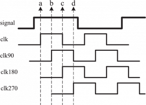
A major demand of over-sampling is that the sampling clock frequency should be an integer multiple of the signal frequency. To make multi-phase sampling clocks, we take help from the digital clock management (DCM) module of FPGA instead of a high-frequency clock. The frequency of sample clocks is thus the same as the frequency of the signal. The sampling of signal occurs at every rising edge of the multiphase clocks for sampling, as indicated in Figure 1, and four sampling clocks with a phase difference of 90 degrees i.e., clk, clk90, clk180, and clk270 may achieve four times oversampling. Excessive jitter in the sample clock might lead to sampling variance.
Sampling values are synchronized
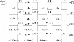
The sampling is implemented in the real circuit by four registers. The registers can be found in the first column in Figure below. The delay we get from the input pin of the signal to every register should be as short as feasible to ensure sampling accuracy. As a result, we should must limit the maximum skew time of the signal, in the time the placement of four registers, above mentioned, used to sample the signal. They should be kept close to the signal’s input pin. The maximum skew time requirement is achieved by a timing constraint, while the sampling register position limitation is realized by an implementation constraint in an FPGA.
The sample values in distinct clock domains are [0], bs[0], cs[0], and ds[0]. It is mandatory that they should be synchronized with the standard clock “clk” before being used to identify transition edges. As illustrated in the diagram below, the synchronous circuit is made up of numerous registers with their trigger clocks varying, and therefore it varies the time delay between neighboring registers. After four registers, a delay is called in the sampling value. The value is delayed by 3T (T is the period of “clk”), resulting as[3], bs[3], cs[3], and ds[3] entirely synchronized with the standard clock. Furthermore, these synced registers eliminate four sampling registers’ meta-stability.
Transition edges of signal are determined according to the sampling values
The transition edges of a serial transmission are easily detectable. All we have to do now is compare all neighboring sample results in a normal clock cycle. We may conclude that the transition occurs between the two sample points that correspond to the adjacent sampling values if there is a difference between the two adjacent sampling values.
Appropriate sampling points are found basing on the information of transition edges
We may determine the best sampling places based on the information from transition edges. An ideal sample point should be in the center of a single bit signal, according to the criteria. As a result, we can come up with the following selection criteria:
- The best sampling point is c, if the transition occurs between d and a.
- The best sampling point is d, if the transition occurs between a and b.
- The ideal sampling point is cycle a. If the transition occurs between b and c.
- The ideal sampling point is cycle b, if the transition occurs between c and d.
- The ideal sampling point is consistent in this cycle with the preceding cycle if there is no transition in the standard clock cycle.
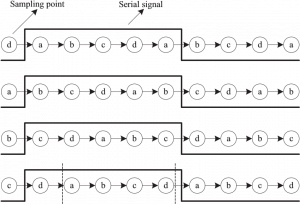
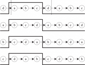
Figure 3 explains that sample clocks are quicker than signal clocks. When the sampling clocks’ frequency is somewhat faster than the signal’s frequency, a single bit signal may be sampled five times over time. In the last row of the above figure 3, there is an unusual circumstance. An entire sampling cycle is contained in a single bit signal. This cycle’s ideal sampling point is the same as the previous cycle, and the following cycle’s b sampling point is the same as the previous cycle. However, having an ideal sample point in this cycle is not required.
Figure 4 shows that the signal is faster than the sampling clocks. When the sampling clocks’ frequency is somewhat slower than the signal’s frequency, a single bit signal may be sampled three times with the passage of time. In the first row of figure 3, there is another pretty rare occurrence. Two transitions take place throughout a sample cycle. In this unique sample cycle, there should be two ideal sampling points, according to the selection principles.
Analysis of Performance
Tolerance of Jitter
As previously stated, jitters in the signal and sampling clocks cause the sampling clocks and signal to be out of synchronization. Jitter is classified into the following two types:
Random jitter
Random jitter, on the other hand, is impossible to anticipate and is supposed to have a Gaussian distribution. Random jitter does not have a finite peak value in principle.
Deterministic jitter
Period jitter, data-dependent jitter, and duty-cycle dependent jitter are the several types of deterministic jitter. The cause and peak-to-peak value of deterministic jitter can be determined.
We have only addressed period jitter in this paper since other jitters are more dependent on real-world applications. To ensure that the optimal sampling points sample the correct signal value, the number of sampling points in a cycle of standard clock “clk” must be greater than or equal to 3 and less than or equal to 5, with the absolute value of the period jitter not exceeding 0.25 T (T being the period of “clk”).
Requirement of Signal
Transition of signals must occur again and again for the strategy to work. In the meantime, one quarter clock cycle is drifted by the sample clock, at least one signal transition is required. One signal period is around 20ns if it is coming at a speed of 50Mb/s. After that, one-fourth of a period is 5ns. If the oscillator of the frequency local receiver is 51MHz, it has a period of 19.608ns, making it (2019.608) =0.392ns quicker than the incoming signal. The quarter time (5ns) multiplied by 0.392ns equals around 13. To work properly, the circuit requires at least one transition every 13 clock cycles. This need will not be a problem in reality if the incoming data is encoded using a method like 8B10B.
Experimental Results
We utilized two FPGA circuit boards to validate the suggested method: one for generating serial signals and the other for receiving them. A connection connects the two boards plus a FPGA chip. For this test, we use a 50Mbps transfer rate serial signal.
The test’s structure is depicted in Figure below. At the transmitter, the PRBS signal is created. The signal is sent to the receiver through the cable. The data is recovered from the PRBS signal by the receiver. The PRBS check module verifies that the recovered data is valid before sending the results to the ‘error statistic module’. The error statistic module’s output signals are known as bit_num and err_num. The count of bits we receive is the bit_num, while the count of incorrect bits is err_num.
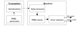
Here bit num and err num shows real-time value, to see that we used the software named Xilinx Chipscope. The Figure below shows the findings, which demonstrate that the error rate is less than 10-12. As a result, our technique may be used in real-world applications.
Conclusion
In this paper, we have drafted and proposed a very feasible method to recover data for high speed serial communication. The major thought and implementation of this method revolves around over-sampling. And we performed and cross checked our method by Verilog language in FPGA. The experimental results and outcomes of simulations demonstrated that this recovery method is practically usable.
Related Topics
-
What are the factors that Influence the selection of Embedded Microcontrollers?
-
How to do the software power optimization in embedded systems?
-
Revolution brought by Embedded Systems with Data Analytics
-
what are the practical applications of embedded systems?
-
what are the challenges in embedded systems design?
-
Discuss the stimulation study of Elevator’s control system
-
Embedded Systems Future: Design of optimized Energy Metering Devices