Shift Registers
What are the universal shift registers and their applications? A shift register is a type of digital circuit using a cascade of flip-flops where the output of one flip-flop is connected to the input of the next. They share a single clock signal, which causes the data stored in the system to shift from one location to the next. By connecting the last flip-flop back to the first, the data can cycle within the shifters for extended periods, and in this form they were used as a form of computer memory. In this role they are very similar to the earlier delay-line memory systems and were widely used in the late 1960s and early 1970s to replace that form of memory.
In most cases, several parallel shift registers would be used to build a larger memory pool known as a “bit array”. Data was stored into the array and read back out in parallel, often as a computer word, while each bit was stored serially in the shift registers. There is an inherent trade-off in the design of bit arrays; putting more flip-flops in a row allows a single shifter to store more bits, but requires more clock cycles to push the data through all of the shifters before the data can be read back out again.
Shift registers can have both parallel and serial inputs and outputs. These are often configured as “serial-in, parallel-out” (SIPO) or as “parallel-in, serial-out” (PISO). There are also types that have both serial and parallel input and types with serial and parallel output. There are also “bidirectional” shift registers, which allow shifting in both directions: L → R or R → L. The serial input and last output of a shift register can also be connected to create a “circular shift register”. A PIPO register (parallel in, parallel out) is very fast – an output is given within a single clock pulse.
What is universal shift register?
A register that can store the data and /shifts the data towards the right and left along with the parallel load capability is known as a universal shift register. It can be used to perform input/output operations in both serial and parallel modes. Unidirectional shift registers and bidirectional shift registers are combined together to get the design of the universal shift register. It is also known as a parallel-in-parallel-out shift register or shift register with the parallel load.
Universal shift register are capable of performing following 3 operations
- Parallel load operation – stores the data in parallel as well as the data in parallel
- Shift left operation – stores the data and transfers the data shifting towards left in the serial path
- Shift right operation – stores the data and transfers the data by shifting towards right in the serial path.
Hence, Universal shift registers can perform input/output operations with both serial and parallel loads.
Diagram:
4-bit Universal shift register diagram is shown below.
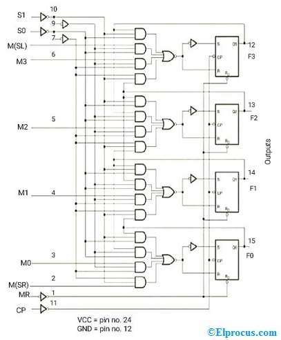
- Serial input for shift-right control enables the data transfer towards the right and all the serial input and output lines are connected to the shift-right mode. The input is given to the AND gate-1 of the flip-flop -1 as shown in the figure via serial input pin.
- Serial input for shift-left enables the data transfer towards the left and all the serial input and output lines are connected to shift-left mode.
- In parallel data transfer, all the parallel inputs and outputs lines are associated with the parallel load.
- Clear pin clears the register and set to 0.
- CLK pin provides clock pulses to synchronize all the operations.
- In the control state, the information or data in the register would not change even though the clock pulse is applied.
- If the register operates with a parallel load and shifts the data towards the right and left, then it acts as a universal shift register.
Design of universal shift register
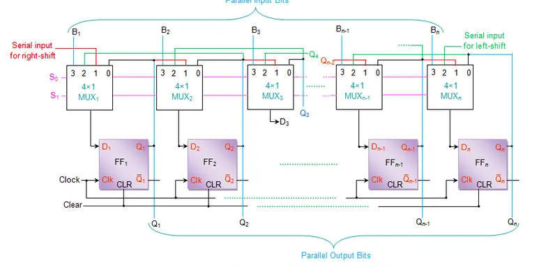
The design shown by Figure 1 uses n 4×1 multiplexers to drive the input pins of n flip-flops in the register which are also connected to clock and clear inputs. All of the multiplexers in the circuit share the same select lines, S1 and S0 (pink lines in the figure), in order to select the mode in which the shift registers operates. It is also seen that the MUX driving a particular flip-flop has its
- First input (Pin Number 0) connected to the output pin of the same flip-flop i.e. zeroth pin of MUX1 is connected to Q1, zeroth pin of MUX2 is connected to Q2 , … zeroth pin of MUXn is connected to Qn.
- Second input (Pin Number 1) connected to the output of the very-previous flip-flop (except the first flip-flop FF1 where it acts like an serial-input to the input data bits which are to be shifted towards right) i.e. first pin of MUX2 is connected to Q1, first pin of MUX3 is connected to Q2, … first pin of MUXn is connected to Qn-1.
- Third input (Pin Number 2) connected to the output of the very-next flip-flop (except the first flip-flop FFn where it acts like an serial-input to the input data bits which are to be shifted towards left) i.e. second pin of MUX1 is connected to Q2, second pin of MUX2 is connected to Q3,… second pin of MUXn-1 is connected to Qn.
- Fourth input (Pin Number 3) connected to the individual bits of the input data word which is to be stored into the register, thus providing the facility for parallel loading.
The design of a 4-bit universal shift register using multiplexers and flip-flops is shown below.
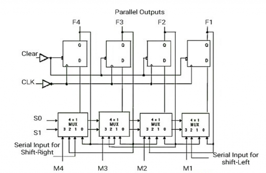
- S0 and S1 are the selected pins that are used to select the mode of operation of this register. It may be shift left operation or shift right operation or parallel mode.
- Pin-0 of first 4×1 Mux is fed to the output pin of the first flip-flop. Observe the connections as shown in the figure.
- Pin-1 of the first 4X1 MUX is connected to serial input for shift right. In this mode, the register shifts the data towards the right.
- Similarly, pin-2 of 4X1 MUX is connected to the serial input for shift-left. In this mode, the universal shift register shifts the data towards the left.
- M1 is the parallel input data given to the pin-3 of the first 4×1 MUX to provide parallel mode operation and stores the data into the register.
- Similarly, remaining individual parallel input data bits are given to the pin-3 of related 4X1MUX to provide parallel loading.
- F1, F2, F3, and F4 are the parallel outputs of Flip-flops, which are associated with the 4×1 MUX.
Working of PIPO registers
- From the above figure, selected pins the mode of operation of the universal shift register. Serial input shifts the data towards the right and left and stores the data within the register.
- Clear pin and CLK pin are connected to the flip-flop.
- M0, M1, M2, M3 are the parallel inputs while F0, F1, F2, F3 are the parallel outputs of flip-flops
- When the input pin is active HIGH, then the universal shift register loads / retrieve the data in parallel. In this case, the input pin is directly connected to 4×1 MUX
- When the input pin (mode) is active LOW, then the universal shift register shifts the data. In this case, the input pin is connected to 4×1 MUX via NOT gate.
- When the input pin (mode) is connected to GND (Ground), then the universal shift register acts as a Bi-directional shift register.
- To perform the shift-right operation, the input pin is fed to the 1st AND gate of the 1st flip-flop via serial input for shit-right.
- To perform the shift-left operation, the input pin is fed to the 8th AND gate of the last flip-flop via input M.
- If the selected pins S0= 0 and S1 = 0, then this register doesn’t operate in any mode. That means it will be in a Locked state or no change state even though the clock pulses are applied.
- If the selected pins S0 = 0 and S1 = 1, then this register transfers or shifts the data to left and stores the data.
- If the selected pins S0 = 1 and S1 = 0, then this register shifts the data to right and hence performs the shift-right operation.
- If the selected pins S0 = 1 and S1 = 1, then this register loads the data in parallel. Hence it performs the parallel loading operation and stores the data.
| S0 | S1 | Mode of Operation |
| 0 | 0 | Locked state (No change) |
| 0 | 1 | Shift-Left |
| 1 | 0 | Shift-Right |
| 1 | 1 | Parallel loading |
From the above table, we can observe that this register operates in all modes with serial/parallel inputs using 4×1 multiplexers and flip-flops.
what are the applications of universal shift registers?
The applications of a universal shift register include the following.
- Used in micro-controllers for I/O expansion
- Used as a serial-to-serial converter
- Used as a parallel-to-parallel data converter
- Used as a serial-to-parallel data converter.
- Used in serial – to – serial data transfer
- Used in parallel data transfer.
- Used as a memory element in digital electronics like computers.
- Used in time delay applications
- Used as frequency counters, binary counters, and Digital clocks
- Used in data manipulation applications.
What are the advantages of universal shift registers?
The advantages of a universal shift register include the following.
- This register can perform 3 operations such as shift-left, shift-right, and parallel loading.
- Stores the data temporarily with in the register.
- It can perform serial to parallel, parallel to serial, parallel to parallel and serial to serial operations.
- It can perform input-output operations in both the modes serial and parallel.
- A Combination of the unidirectional shift register and bidirectional shift register gives the universe shift register.
- This register acts as an interface between one devices to another device to transfer the data.
Also read here
https://eevibes.com/digital-logic-design/what-are-the-modern-digital-circuits/