
Overview
Atomic Silicon Quantum Dot and Atomic Logic Design. Silicon has a vast role in the field of Electronics. Silicon Quantum Dots (SiQDs) are the semiconductors Si nanoparticles, within the range of 1nm to 10nm. They can emit red and blue light which makes them very useful as optoelectronic devices and fluorescent biomarking agents. The main factor is that the biocompatibility of silicon atomic dots is compared to the conventional toxic metal dots of Group II-VI and III-V. The silicon quantum dot consists of a Dangling bond. The recent progress work in logic circuits using atomic-scale silicon dangling bond (DB) makes it a promising candidate in the field of coupled nanocomputing. This arising innovation is still in its underlying stage. This paper presents a T-shape construction to acknowledge logic circuits. Moreover, essential logic gates, for instance, two-input AND gate, NAND gate, OR gate, XOR gate and XNOR gate, are accounted for utilizing the T-shape structure. Besides, a novel three-input majority (Si-DBM3) gate and a three-input XOR (SiDBX3) gate, based on dangling bond pairs, have been introduced. Using the proposed Si-DBX3 and Si-DBM3 logic gates, a Full-adder circuit is designed.
Background
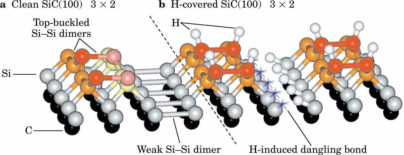
Silicon dangling bond DBs are fabricated by desorbing a single hydrogen atom from a hydrogen-terminated silicon surface using a scanning tunneling microscope (STM) probe. By applying a voltage pulse to the hydrogen site, the H-Si bond is broken, leaving a valence orbital.
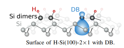
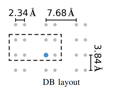
The hydrogen sites are located on silicon atoms, the sites are discretely defined by the lattice structure, and DBs can be created at atomically precise locations as shown in the figure below.
There are three skim states a DB can hold. An unoccupied positive state (DB+), a singly occupied neutral state (DB0), and a doubly occupied negative state (DB-).
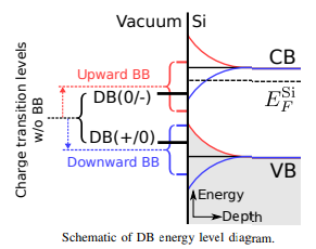
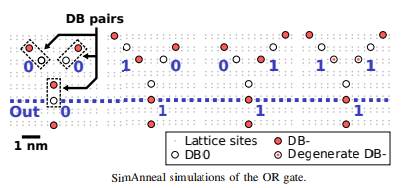
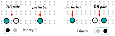
They are believed to be electrically decoupled from the bulk, allowing discrete electron populations by manipulating the relative energy positions between the Fermi energy and charge transition levels of the bulk. Several factors contribute to the band bending, such as the contact potential of the nearby STM or atomic force microscope (AFM) tip and the Coulomb interactions between the DBs with external fields such as charged subsurface dopants. This band bending shifts the charge transfer level concerning the bulk Fermi level. When the change in energy situation causes the charge transfer level of DB to exceed the Fermi level, the charge number of DB changes. Local charge defects or dopants can influence the energy at which this occurs through proximity-based gating effects. The potential of DBs as building blocks of computer logic circuits has been demonstrated before when a binary OR gate consisting of three radially arranged DB pairs was proposed, as shown in the figure below.
Also check :What are the Quantum Dots?
Each DB pair carries one bit of information about the position of the negative charge within it. The input logic state is enabled by the presence of a disturber, which is a peripheral DB energetically preferred to remain in the DB state regardless of the state of other DBs in the circuit. The output comes from the load status of a particular DB. Charge states were measured using AFM to relax the system to the ground state. Furthermore, non-equilibrium charge dynamics were studied by AFM experiments on a 6-DB structure designed to be energetically frustrating such that electrons tend to localize to one of the innermost DBs. . Scanning the structure, we observed electron ‘hopping’ between these sites, with each localization persisting over multiple line scans. We were able to simulate the ground state and frustration ground state jumping phenomena. The potential for building nanometer-scale logic circuits from atomic DBs makes this technology a promising candidate for further circuit miniaturization and power reduction research. Additionally, using a silicon substrate opens up opportunities to integrate his DB circuits into the existing infrastructure of silicon complementary metal-oxide semiconductor (CMOS) devices. This is a new design space with largely unknown design rules and constraints. More logic gates and circuit components await investigation. The SiQAD project aims to lower the barriers for the research community to explore this platform technology and develop design rules that can effectively design complex circuits and systems at the atomic level.
What are the Applications of Quantum Dots?
Introduction
In recent decades, researchers have made great strides in the field of nanotechnology, which has the potential to exceed the capabilities of complementary metal-oxide semiconductors (CMOS). Several projects and demonstrations towards quantum dot electronics, molecular electronics and atomic electronics have been reported. Among all these emerging technologies, quantum dots have become very important as they have managed to remain smaller, faster, consume much lower power, and have higher functionality than existing CMOS technologies.
Silicon is widely used in electrical devices, but there are few optical applications for bulk silicon. Silicon quantum dots are extremely small (Nano-sized) particles of crystalline silicon with properties for a wide range of applications in microelectronics, photonics, and biotechnology applications. The production of Nano-sized silicon particles can be divided into chemical and physical processes. The first is laser ablation and non-thermal plasma synthesis. The second is an electrochemical etching, reduction of silicon halides, thermal destruction of silicon-rich oxides, hydrothermal decomposition of various organic elements including Si, and mechanochemistry.
What is the Quantum dot?
These are perfect implementations of quantum mechanics in the field of semiconductors. The size of these particles is usually in nanometers and the special quality which they possess are optical and electronic properties that are unique and differ from large particles. These quantum dots form the basis of nanotechnology. When a high-energy UV light falls on the quantum dots, these dots get excited enough to go to a higher energy state. In the case of semiconductors, this process can be stated as when energy is received by these dots, they elevate themselves from the valence band to the conduction band. The excited electron then returns to its original valence band; it follows a release of energy. This light energy can be visible to the naked eye if it falls in the visibility range of the eye. The color of the light mainly depends upon the energy gap between the valence band and the conduction band.
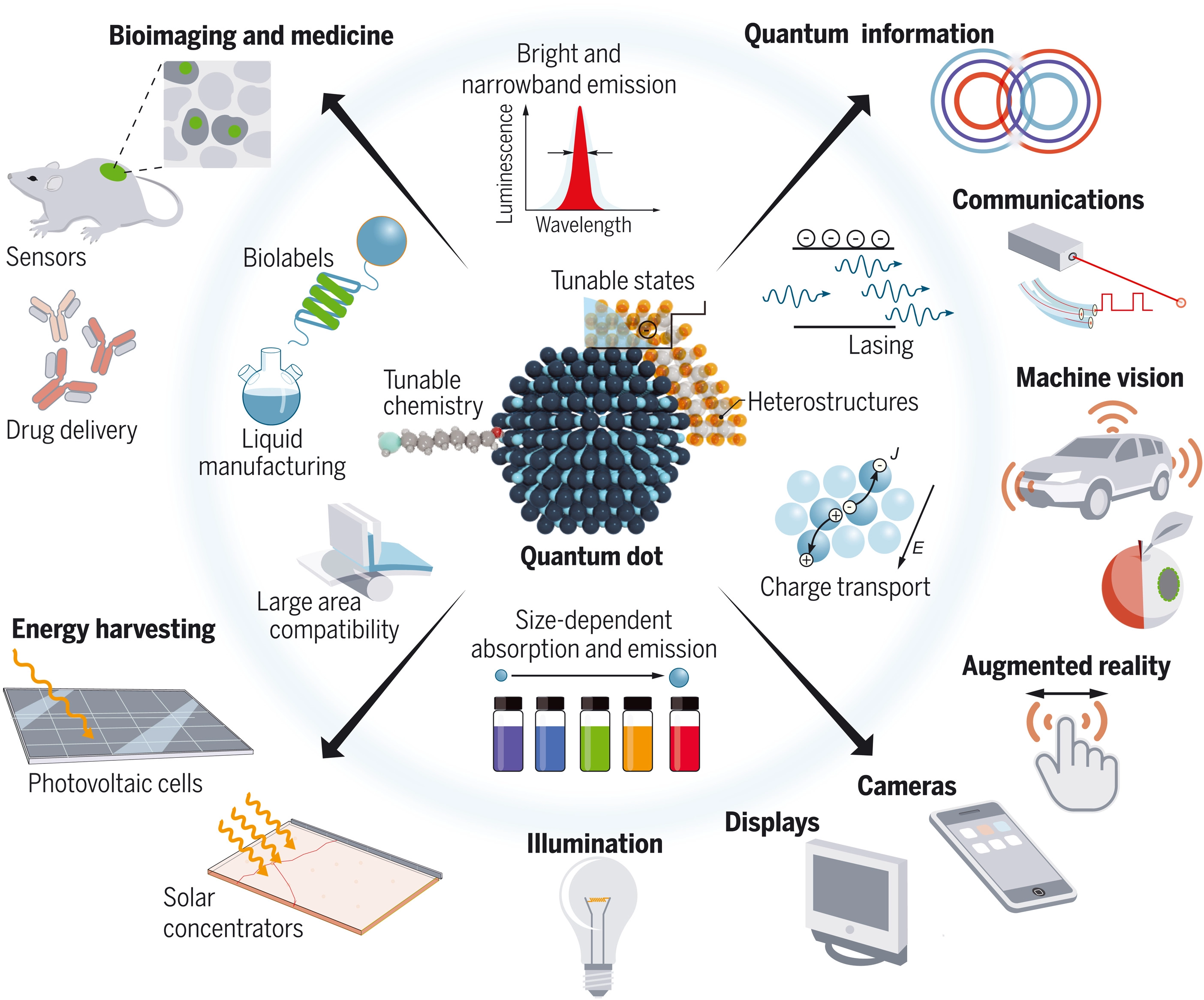
In materials science, nanoscale semiconductor materials confine electrons or holes. Here, these quantum dots are commonly called artificial atoms. They combine individual electronic states like naturally occurring atoms and molecules. Artificial molecules can be made by combining two or more quantum dots, which also exhibit hybridization at room temperature.
The optoelectronic properties of quantum dots change according to time. Larger QDs of usually 5-6 nm diameter emit longer wavelength. However, the emission of different colors varies depending on the composition of QD.
Define Dangling bond
A dangling bond is an unsatisfied valence electron on an immobilized atom. It is also referred to as immobilized free radical or immobilized radical. Dangling bonds having one valence electron leads to a neutrally charged atom. If the valence electrons are two, the energy of the dangling bond is near the valence band. Whereas, zero valence electrons lead to a condition where the energy of the dangling bond is similar to the conduction band.
In hydrogenated silicon, dangling bonds can be induced by long exposure to light. Long exposure to light will cause a decrease in the photoconductivity of the material (Staebler-Wronski effect). The mechanism of this can be explained. The photon energy is used to break the bond between Si-Si. This leads to the formation of two new radicals. The radicals then try to remain in the most stable state which can be achieved when hydrogen moves to the point of bond breakage and the valence move far apart. The electrons get further delocalized. It is observed that by increasing temperature, the rate of formation of light-induced dangling bonds will also increase. Thus temperature also plays a plus factor in this regard. This process can be simplified by increased hydrogen diffusion.
SiQAD Overview
SiQAD is a CAD tool that enables the design and simulation of DB circuits via an intuitive graphical user interface (GUI) and modular simulation backend. The GUI is written in C++ using the Qt cross-platform application framework and provides tools for DB layout design, simulation management, and multi-layer electrode placement. SiQAD GUI communicates with the simulation engine through a custom simulation application programming interface (API). Simulation engines can use this API through a provided class structure that supports engines developed in C++ or Python. The general flow of the simulation when invoked by the user is:
- SiQAD exports a file containing the simulation parameters as well as the DB and electrode designs
- The desired simulator is invoked with user-configurable command line arguments
- Result files generated by the simulator are read and parsed by SiQAD, with supported result types displayed in the GUI.
Currently supported result visualization types include DB state-of-charge configuration and electrostatic landscape results. The simulation engine can also instruct SiQAD to perform design actions such as creating, moving and deleting design objects through the instruction API. The first version of SiQAD contains three simulation tools, whose features and capabilities were described in the previous section. Additional engines can be implemented and integrated through the provided API. Open-source tools allow the research community to modify or provide additional functionality, supporting the future growth of SiQAD as a platform for designing DB circuits.
Simulation Engines
The first release of SiQAD officially included three simulation engines, each with a different purpose and functionality as described below.
- SimAnneal: simulated annealing algorithm for finding metastable low energy charge configurations.
- HoppingDynamics: non-equilibrium electron hopping dynamics simulation intended for capturing the experimentally observed hopping behaviour.
- PoisSolver: electrostatics solver which solves the generalized Poisson’s equation to find the electric potential landscape arising from clocking electrodes in the system.
Proposed Logic Gates
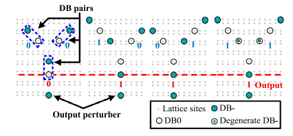
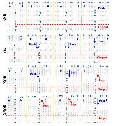
DB-based atomic-scale logic design is a new technology area with many designing ways. Here, we use the T-shaped design rule to achieve two-input atomic AND, NAND, OR, XOR, and XNOR gates. We use SiQAD and SimAnneal simulation engines to design and verify the proposed gates.
SiQAD helps detect logic gates by altering input/output pattern interference sources and altering the distance between idle connections. A perturbator is an I/O control key that acts as an enabler. Her four sides of the grid are spaced apart to achieve AND gates, DB pairs and output disturb bars. Four grid-site DB pairs and five grid-site output interferer isolation are used for OR gates. Similarly, other logic gates can be constructed by varying the spacing of DB pairs and output disturbers.
In Nano computing, the majority of gate-based logic becomes more popular than the traditional AND, NAND, OR and NOR gate-base logic. The three-input majority gate is the most potent logic block and is widely used in designing different logic circuits. the hardware cost of these three input majority gates is the same as basic compound logic AND-OR-Invert (AOI) gates.
In nano-computing, one of the biggest challenges in circuit design is wire crossing. Three types of wire crossing
- Clock-Zone-Based
- Rotated Cell-Based
- Multilayer
These are very common in QCA. However, in atomic silicon technology, there is no evidence that this technology can support multi-layer and twist-cell-based wire crossings. Wire crossings are therefore one of the biggest design challenges in atomic silicon technology. Here we use a new technique to solve this problem in a single-layer structure. This method allows different signals to cross from any direction. 4 Disruptors are placed in 4 directions. north, south, east and west so that the proposed structure forms exactly a rhombus called “coplanar rhombus” as shown in the image below
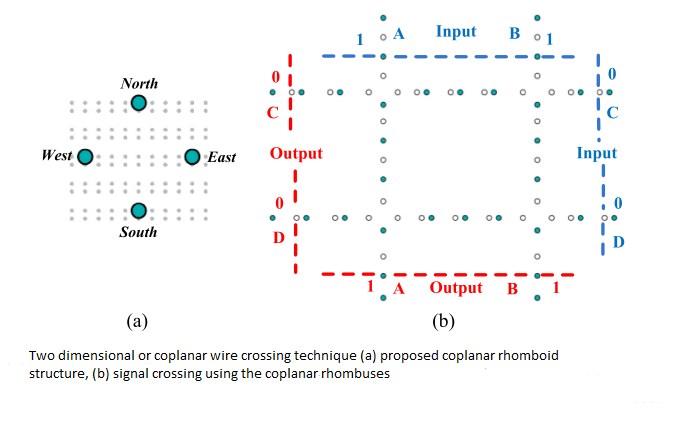
the four inputs A, B, C, and D use four coplanar rhombus structures to cross each other. All input signals are successfully crossed and measured at the output terminal.
Proposed Full-Adder
Using the proposed basic logic gates, a 1-bit full adder (FA) based on DB logic was realized for the first time, as shown in FIG. To minimize design complexity, the proposed new Si-DBM3 and Si-DBX3 were used in place of his AOI logic gates. The sum bit is calculated using only one i-DBX3 gate and the carry bit is implemented using only one SiDBM3 gate. This is easily understood using the following formula:
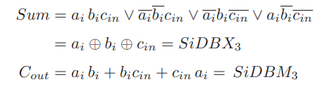
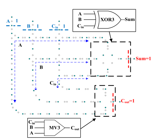
Here, ai, bi and cin are three arbitrary inputs, and Sum and Cout are the two outputs. The proposed 1-bit FA is designed and simulated using SimAnneal by considering the environmental factors of µ− = −0.28 eV, ϵr = 5.6, and λTF = 5 nm. Here, µ− is the energy difference between (0/-) charge transformation energy and the bulk Fermi energy. To attain a compact circuit layout, a high empirical potential environment is considered. Moreover, to avoid the closed-loop condition, the proposed wire-crossing technique is used.
Results
The proposed design was validated using the SiQAD simulation tool with the default simulation settings of the SimAnneal engine. The frequency column shows the accuracy of the logic gate given various input combinations. Here input states 01 and 10 are identical due to symmetry. Therefore, only state 01 is considered. It turns out that logic blocks are more likely to occur in true conditions most of the time. Moreover, all designs are physically valid for all input configurations, indicating that the proposed T-shaped logic block is valid. The probability of the true state occurring is similar for the Si DBM3 and Si DBX3 gates.
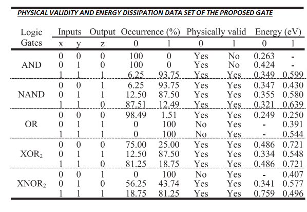
Using the SimAnneal simulation engine, we vary the physical parameters ϵr and λTF to determine the charge regeneration capability of the proposed gate. For any input configuration, all proposed gates exhibit a large continuous operating window at μ− = −0.28 eV. This is highly desirable. The wide operating range indicates that the proposed design rule is robust over a wide range of physical surface parameters.
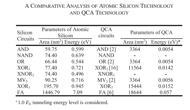
Table II provides an overview of atomic silicon and QCA techniques. For atomic silicon, we only consider the high input states (11 for 2-input gates and 111 for 3-input gates). Compared to QCA circuits, atomic silicon-based circuits are much smaller. However, QCA circuits consume much less power. The power consumption of QCA circuits is estimated using his QCA Pro tool, which considers non-adiabatic clocking schemes and evaluates only the upper bound of power consumption. This is a possible reason why QCA circuits exhibit lower energy dissipation than atomic silicon.
Conclusions
Recent advances in DB quantum dot technology show its potential in atomic-scale logic design. In this thesis, we have proposed a T-shaped design layout to implement binary logic on the silicon database platform. By combining basic logic blocks, we designed a one-bit full adder, which is the largest Si-DB-based logic circuit to date. The SiQAD simulation tool is used to design and verify the proposed design. All proposed building blocks exhibit higher real state probability and wide operating windows, which demonstrates their robustness and physical value. These gates will serve as reference building blocks in the design of more complex DB-based circuits in the future. Also, one thing to keep in mind is that this technology is not yet adopted but the time will come when it will prove itself to users and handlers.
Also read here: