
Introduction
In this article we have discussed about the Design of Analog to Digital Converter Using CMOS Logic. The biggest advantage in Digital circuits and digital signals as compared to analog circuits and signals is the processing speed and efficient transmission. The comparator is the most important component in the ADC architecture. In Flash ADC, it is possible to achieve higher speed, linearity, accuracy and high resolution. Furthermore, the Fat Tree Encoder can be used to double up the speed of Flash ADC.
The minimum channel length of the transistor will be scaled down to 0.065 um in 2007, according to the Roadmap of semiconductors. In addition to this downscaling, today’s system-on-chip (SoC) trend forces analog and Digital integrated circuits (ICs) to be integrated on a single chip called the complete SoC ADCs for the complete SoC are high-speed conversion, low-power dissipation, and low-voltage operation. In Terms of high-speed conversion, 0.13 um CMOS technology presently allows processor speeds in excess of 2.4 GHz. However, the sampling speed of ADCs fabricated with an advanced process has been around 200 mega Samples per second (MSPS).
To remove the speed gap between a processor and an ADC in the complete SoC implementation, an ADC architecture must not only be fast but also cheap. Another challenge is Low-Power dissipation. The down-scaling of the minimum channel length to 0.065 m results in the reduction of the power supply voltage to 0.7 V. As a result, an ADC should be operated in a small voltage range.
-
SOLID-STATE TECHNOLOGY
Three Different types of solid-state technologies are currently used for high-speed ADC implementations: CMOS technology, bipolar technology, and Gallium Arsenide (GaAs) technology. GaAs technology is the fastest of the three, and CMOS technology is the slowest. Since BiCMOS is much more expensive than CMOS technology, mixed-signal circuit implementation using only the standard CMOS technology is the preferred choice for SoC products.
-
Proposed System- THRESHOLD INVERTER QUANTIZATION (TIQ) Flash ADC
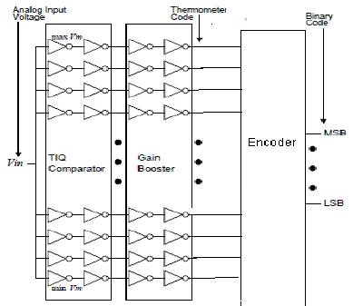
We propose a high-speed CMOS Flash Analog to Digital Converter architecture with low power dissipation, which features the Threshold Inverter Quantization (TIQ) technique. The main advantage of the TIQ based CMOS Flash Analog to Digital Converter (TIQ Flash Analog to Digital Converter) design is a simpler comparator design. The idea is to use digital inverters as analog voltage comparators. This eliminates the need for high-gain differential input voltage comparators that are inherently more complex and slower than the digital inverters.
-
TIQ Comparator
The TIQ comparator compares a reference voltage Vref with input voltage Vin and convert Vin into 1 or 0. If Vin is greater than Vref, the output of the comparator is 1 otherwise 0.
Commonly used comparator structures in CMOS ADC design are the fully differential latch comparator and the dynamic comparator . The former is sometimes called a clocked comparator,” and the latter is called an auto-zero comparator” or chopper comparator.” To achieve high speed, such comparators are usually implemented with bipolar transistor technology.
-
Gain Boosters
It uses two cascaded CMOS inverters as a comparator for high speed conversion and low power dissipation.
-
TC to BC Encoder
The thermometer code to binary code (TC-to-BC) encoder typically converts the thermometer code to a binary code (BC) in two steps after the comparators have produced the TC. XOR logic is used to change the TC into the 1-out-of-n code. After that, this code is changed to BC. Top speed the glimmer ADC, we propose a new TC-to-BC encoder named as the fat tree encoder that is profoundly reasonable for a high velocity and low power CMOS streak ADC.
-
Fat Tree Encoder
To speed up the encoder, which is a bottleneck in the speed of a flash ADC, we suggest using the fat tree encoder[2]. The fat tree encoder outperforms other encoders primarily due to its fast encoding speed and low power consumption. The fat tree encoder’s sign deferral is 0(log2N) on account of its tree engineering. As a result, it runs much faster than an encoder of the ROM variety; for instance, in 3-bit encoding, there are only two OR gate delays. One of the obstacles to enhancing the TIQ flash ADC’s implementation is the fat tree encoder’s three-dimensional design automation.
Simulation Results & Discussions
The TIQ flash ADCs’ circuits and experimental findings are discussed here. The TIQ flash ADCs were developed using the ADS 2004A tool and standard CMOS technology [4] at 130 nm. The HSPICE models have been utilized as the standard library.
-
Threshold Values
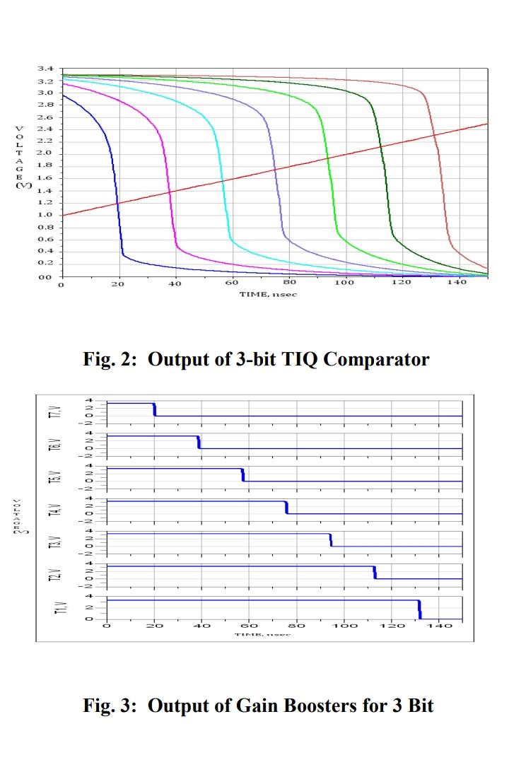
As depicted in Fig. 1, the threshold voltages (Vm) of the inverter shift with transistor size [7]. Fig. 2 depicts the results of a 3-bit TIQ comparator simulation. The uniformity of seven equally spaced inverter threshold voltages is also depicted in this figure. Table 1 displays the various threshold voltages that were obtained for a step size of 0.1875V and three bits.
Conclusion
The Threshold Inverter Quantization (TIQ) technique is a fast, simple, and cascaded CMOS inverter comparator used in a flash ADC architecture. For advanced TIQ flash ADCs, a new type of encoder known as a fat tree encoder has been developed. The TIQ flash ADC is highly suitable for the complete SoC integration using the standard digital CMOS process due to its higher data conversion rates and comparable power consumption. According to the results of the simulation tests, the fat tree encoder was faster than the standard ROM type encoder.
Also read here: