Soldering Processes
What are the Soldering Processes of Printed Circuit Board (PCB)? There are two main purposes of soldering in PCD designing:
- To provide electrical connectivity between the leads of components an PCB traces.
- To attach components physically to PCB.
There are two general methods of soldering:
- Mass soldering
- Directed Energy
In mass soldering, different types of reflows are included that are : conduction, oven , wave and vapor rephrase. While directed energy includes Lasor, hot gas, iron, hot bar and pin point torch). I will be discussing very few types of these like manual soldering, wave soldering etc.
What is Manual Soldering in PCB?
Manual soldering can be used at any level of applications. Either you want to use it for complete PCB assembly or just to do the repair or touch-up tasks, you can use this method. Different types of manual soldering tools are available. They include soldering irons, hot-air pencils, and induction coils. But they are not necessarily bound to them. One of the drawbacks of manual soldering is it has slow soldering speed. Other than that there is increased risk of electrostatic discharge and during handling process and thermal gradients.
Thermal gradients are usually caused by localized heating and board parts. There is no special layout consideration is required when parts are placed and soldiered manually.
What is Wave Soldering?
In wave soldering process the board is held by its edges on the fluxed, conveyor. and preheated as shown in the figure below.
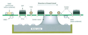
So that only the bottom side of the board is exposed to the solder, the conveyor slides the board past a standing wave of molten solder. It can be used for both through-hole devices (THD) and SMDs but usually we prefer reflow for SMDs. The prefluxed board is arranged with the through-hole components on top and the leads sticking out the bottom. Solder wicks up the barrel and forms fillets on the top and bottom as the conveyer brings the PCB into the solder wave.
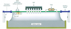
SMDs are run through the boards after being glued and fluxed. If you use very small components or very large tantalum caps for wave soldering then it can be problematic.
During the gluing process, smart parts cause problem as sometimes the glue dots are larger than the component which may result glue to ooze over the solder pads.
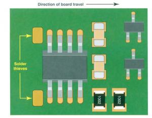
Thermal stresses that can lead to components cracking are caused by large SMDs which is actually a big problem. When we solder the surface mounted devices, the designer should know the direction of board the wave will travel through. The following figure shows how components should be placed on board. It must be kept in mind that the smaller parts should not be shadowed by the larger parts which may result in poor soldering on smaller parts.
Some of the fine leads pitch of some SMDs can cause solder bridging. As each pin leaves the solder wave it tends to draw some of the solder from pin beside it as the molten solder attempts to reduce its surface tension. Due to the lack of pins to draw the extra solder away from the last two rows of pins, which can lead to the last two pins on a side being bridged by the extra solder, this causes a problem.
One way to reduce the bridge is to place solder thieves on SMDs ICs thrilling edges. The extra pads positioned behind the final pads are known as the “solder thieves,” and they serve to remove excessive solder from the pads.
Simply enlarging the final pads and stretching them further back than the rest of the device’s pads will yield a solder thief. Fan-out vias need to be placed away from lands in order to stop solder from migrating from SMD lands and down into the via if SMD parts are on top of the board and are reflow soldered before being wave soldered.
This can happen when heat conducts from the solder wave up via barrels, re-reflows the solder, and then uses capillary action to pull the solder down the via. The recommended distance (1PC-735 I, Section 3.4.6.2) between the vias edge and the pad’s edge is 20 mils. Depending on the parameters, Layout’s default spacing ranges from 50 to 75 mils. There are some boards that might be too big or too small to wave solder.
Without proper holding fittings, large boards sag when they are heated. In order for very small boards to be handled by automated equipment without the requirement for custom board holders, they may need to be panelized with breakaways (tab routes or V scores).
Reflow Soldering
There are many different types of reflow soldering but in this article I will preferably be discussing about oven-type reflow soldering. Surface mount devices mostly use reflow soldering. But it also be used for soldering through-hole components. The schematic diagram of reflow soldering is shown below
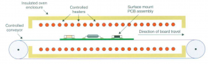
A stencil is used to apply solder paste, which is a viscous paste made of solder and flux. The components are positioned so that the leads sit in the solder paste (often using pick-and-place equipment). A conveyor is used to move the assembly through a temperature-controlled oven, which evenly warms the boards and components. The flux is activated and the solder reflows when the assembly heats up (melts).
The pieces typically self-align due to the molten solder’s surface tension. The component, however, might stand up on one end if parts are not aligned properly and temperature gradients do not melt the solder on all pads at once (called tombstoning). The assembly exits the oven and is cooled to solidify the solder once it has reached the right temperature and the solder has reflowed.
It is necessary to choose solder-able components for both wave and reflow soldering. Additionally, it’s crucial to avoid positioning all of the thermally dense components in one location on the board as this could result in heat gradients across the board and poor solder joint formation in the cooler regions.
Also read here