Introduction to system
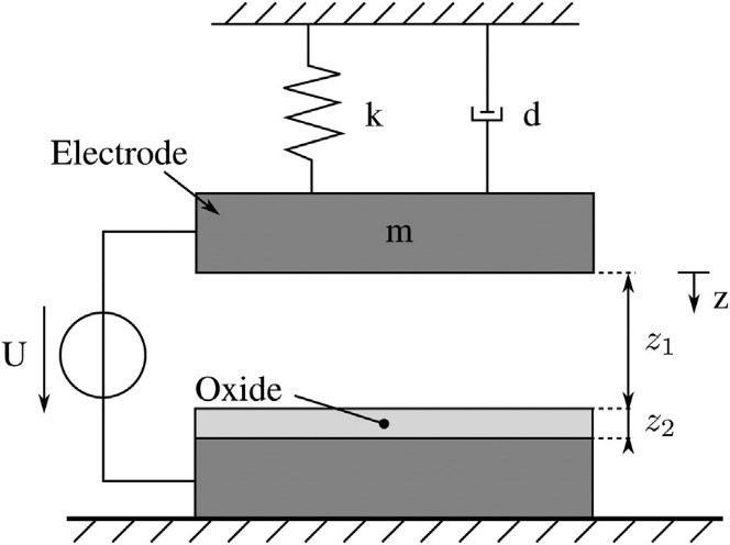
In this article, I have discussed MEMS relay for high power applications. The performance of permanent magnet synchronous motors is defined by their operating range, which is represented by a torque-speed curve. Also, since most of these components are not four-quadrant, they must be doubled to ensure current flows in both directions. In our case, electrostatics is chosen for its low energy consumption and fast response time, ease of integration and also taking into account the magnetic and thermal environment in which the relay will be placed. In terms of energy density, electrostatic relays outperform magnetic relays if the air gap is less than 2 m.
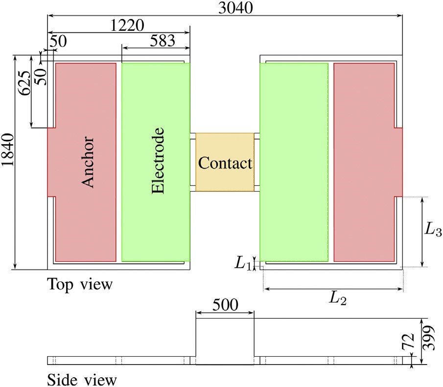
Interest in electrostatically actuated MEMS relays for high performance applications has increased in recent years. The main problem with the design of an ohmic relay is that its inherent resistance creates Joule losses (power dissipation losses) when currents flow through it. It is possible to add an insulating heatsink or to play with the geometry of the structure to have a heatsink integrated into the relay. The proposed relay is based on a two-stage spring system or Cable structure that allows the relay to increase the contact force while remaining within a 5 mm3 volume restriction for integration
Methodology
The literature shows two main trends in MEMS relay manufacturing: sacrificial layer or wafer bonding. Thermo-compression combines the advantages of mechanical and electrical connections between the two wafers in a single structure and is therefore among the many options of joining techniques (direct silicon bonding, anodic bonding, eutectic bonding, glass frit junction, glued). The base substrate is a Boro-float wafer, on which the lower electrodes, electrical conductive tracks, and bonding tracks are produced. Once the two wafers have been thermocompressed, the back of the SOI is finally structured and dry etched to reveal the structures.
Next, a thin layer consisting of a 20 nm adhesive layer of titanium (Ti), a 500 nm seed layer of gold (Au), and a 20 nm protective layer of Ti is deposited. To grow 5 meters of gold within the resistance patterned cavities, an open ring is left around the circumference of the wafer. Due to contamination restrictions during the final post-etch of the SOI, a TiPt peel is performed. A layer of silicon oxide (SiO2) with an adhesive layer of titanium is sprayed onto the wafer to avoid direct contact between the upper and lower electrodes.
For the anchor to be higher than the busbar and electrodes, the top of the wafer must be etched. A wet etching is chosen to ensure an electrical connection between the upper and lower plateau. After removing potassium residues and the hard SiO2 mask, a new thermal oxidation is deposited for electrical insulation, followed by the deposition of the TiAuTi seed layer. For boro-float, 5 meters of gold are grown in a 15meter thick photoresist cavity.
Electrical traces are generated by etching the exposed seed layer, followed by etching with SiO2. To create the moving structure, the upper silicon of the SOI is etched at 87 m and the buried oxide 2 m thick is also removed. When the two wafers are ready to bond, piranha cleaning is carried out to remove organic residues and obtain a high-quality bonding surface. The framework release process can begin by dry etching the back of SOI.
Finally, a silicon oxide dry etching is performed to remove any remaining oxide residue to get the relay enabled.
Conclusion:
We have proposed the design of an electrostatic MEMS relay working in harsh environment and presenting a low contact resistance fulfilling the requirement of electromagnetic motor. Since the contact resistance depends on both the contact surface and force, a two spring (or crableg) structure is used. The proposed design also ensures the flatness of the contact to overcome the main disadvantage of such a structure. This relay has been manufactured using standard cleanroom microfabrication techniques.
The process flow is composed of 18 main steps combining two initial wafers. Electromechanical tests validated the design and the new manufacturing process with a contact resistance of up to 64 m with an applied force of 5 mN. It thus confirms the possibility of integrating a MEMS relay of this type in a permanent synchronous motor and expanding the operating range of said device.
In light of the work already done, several improvements can be suggested. The high enough voltage to activate the relay can be easily reduced by reducing the thickness of the silicon top layer to 72 m instead of 93 m, which reduces the overall stiffness of the relay and possibly a 30 V activation voltage is achieved; a common value for the power supply of an electromagnetic motor. The last value would be the lowest trip voltage ever published for such a low contact resistance. The impact of contact can degrade it over time and eventually lead to failure.
Future work:
Replacing gold by tungsten or ruthenium in one of the two power supply lines will give better stability over time and less stiction problems without increasing the contact resistance too much. So they will be eyeing to do it in near future.
Also read here
https://eevibes.com/electromagnetic-field-theory/what-is-milikans-oil-droplet-method/