SPLDs, CPLDs Vs FPGA
In this article I will discuss General Structure of Field Programmable Gate Arrays. A wide range of logic circuits can be implemented using the 7400 series, SPLDs, and CPLDs. With the exception of CPLDs, these devices are small and only appropriate for simple applications. Only moderately so for CPLDs. A single chip can contain huge logic circuits. In terms of price and performance For these reasons, it’s best to design a desired logic circuit using the fewest available chips. The amount of circuitry on a chip and its functional capabilities are both essential considerations.
To calculate the size of a circuit, assume it will be built using only simple logic gates, and then calculate the number of gates required. A widely used metric is the total number of two-input NAND gates required to construct the circuit. The number of equivalent gates is a common term for this parameter. The size of a 7400-series chip can be easily measured using the equivalent-gates metric. The standard measure for SPLDs and CPLDs is that each macrocell represents around 20 equivalent gates. Thus, a conventional PAL with eight macrocells can support a circuit with up to 160 gates, whereas a huge CPLD with 500 macrocells can support circuits with up to 10,000 equivalent gates.
A circuit with eight macrocells can accommodate up to 160 gates, and a circuit with eight macrocells can accommodate up to 160 gates. A big CPLD with 500 macrocells may implement circuits with up to 10,000 equivalent transistors gates.
Field Programmable Gate Arrays
A logic circuit with 10,000 gates is small by today’s standards implementation. When working with larger circuits, it’s easier to use a chip with more logic capability. A programmable logic device (PLD) is a field-programmable gate array (FPGA). Logic circuits that are relatively large are implemented. FPGAs are not the same as SPLDs. Because FPGAs lack AND and OR planes, they must rely on CPLDs. Rather, FPGAs offer implementation logic blocks for the required functions.
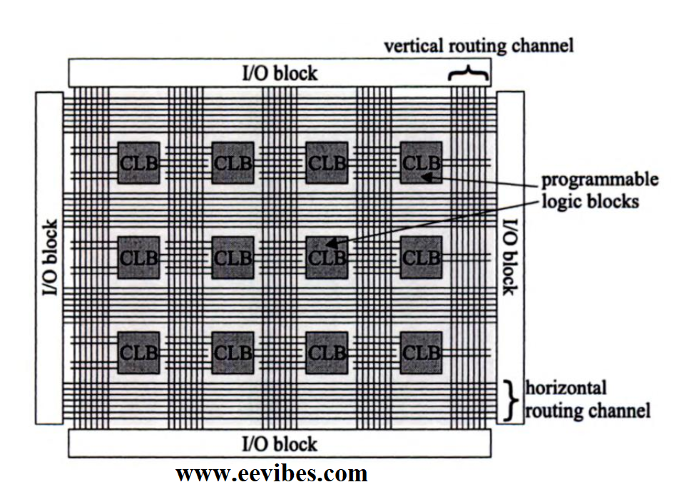
An FPGA’s general architecture figure below illustrates this. It has three categories of resources: logic blocks, I/O, and storage. Interconnection wires and switches, as well as blocks for connecting to the package’s pins. The connectivity cables and logic blocks are placed in a two-dimensional array. Between rows and columns are grouped as horizontal and vertical routing channels Blocks of logic Wires and programmable switches are included in the routing channels. The logic blocks can be joined in a variety of ways.
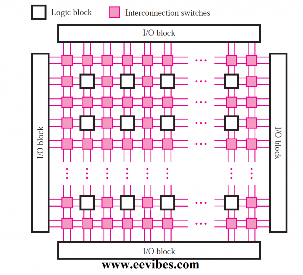
Above figure depicts two locations for programmable switches; the blue boxes next to the logic blocks include switches that connect the logic blocks. the blue boxes, the logic block input and output terminals, and the connector wires that connect one connector wire to another (such as those diagonally between logic blocks) as a horizontal wire to a vertical wire). There are programmable connections between the Interconnection wires and I/O wires. The number of programmable switches in use and wires vary in commercially available chips in an FPGA.
More than a million logic circuits can be implemented using FPGAs. Size of gates Commercial FPGA products from Altera and Xilinx are examples. FPGA chips are available in a variety of packages, including the PLCC and QFP packages described previously in Appendix E. Another sort of packaging is shown in figure below which is referred to as a pin grid array (PGA)
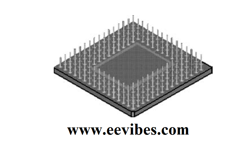
A PGA package might contain hundreds of pins, total, which extend in a grid pattern straight outward from the package’s bottom. Yet the ball grid array is another packaging method that has emerged (BGA). The BGA is similar to the PGA except that instead of posts, the pins are little round balls.
The advantage of BGA packages is that the pins are tiny, allowing for more pins to be packed into a small container. An FPGA logic block usually has a minimal number of inputs and outputs. A wide range of FPGA products are available, each with its own set of logic blocks.
What is LUT?
A lookup table (LUT) is the most common logic block, and it consists of storage cells that are used to implement a tiny logic function. A single logic value, either 0 or 1, can be stored in each cell. The stored value is produced as the storage cell’s output. LUTs of varying sizes can be built, with the number of inputs determining the size. The structure of a tiny LUT is shown in Figure below. It has two x1 and x2 inputs and one f output.
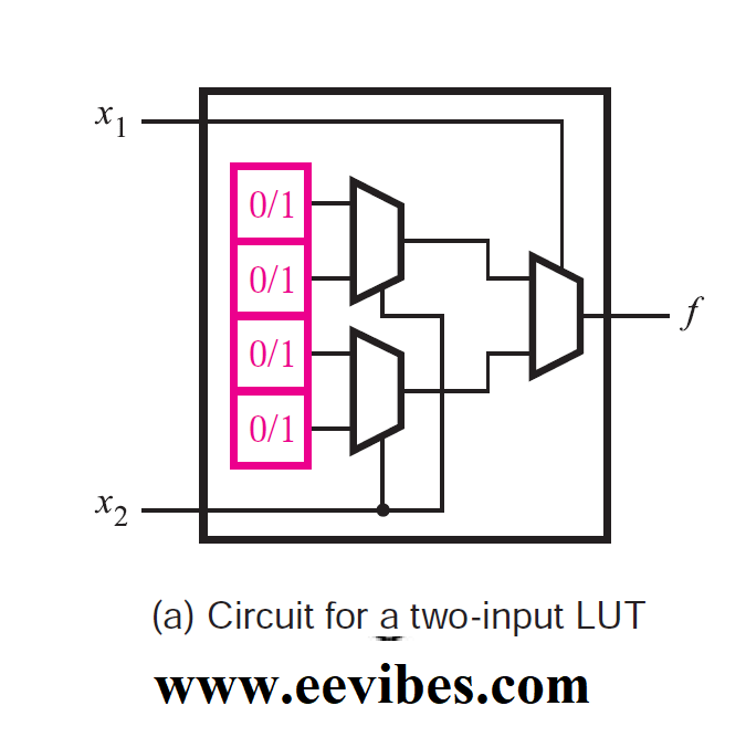
It is capable of implementing any two-variable logic function. This LUT contains four storage cells since a two-variable truth table has four rows. Each row of the truth table has one element that corresponds to the output value. The select inputs of three multiplexers are the input variables x1 and x2, which, depending on their values, pick the content of one of the four storage cells as the LUT’s output.
Consider the truth table in Figure below to show how a logic function can be represented in the two-input LUT. This table’s function f1 can be saved in the LUT as illustrated in figure below.
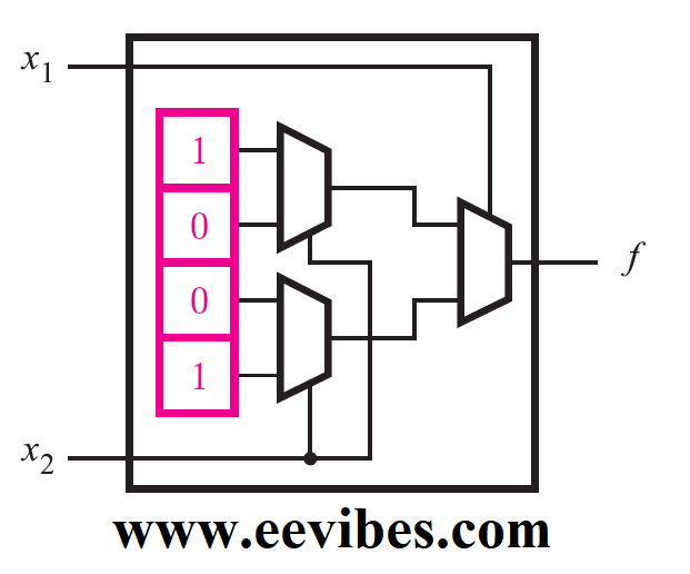
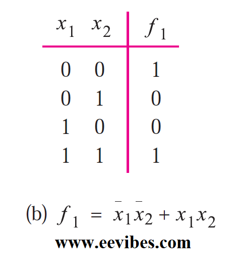
The LUT’s multiplexer design appropriately achieves the function f1. When x1 = x2 = 0, the top storage cell, which represents the entry in the truth table for x1x2 = 00, drives the LUT output. Similarly, the logic value stored in the storage cell corresponding to the item in the truth table chosen by the particular valuation appears on the LUT output for all valuations of x1 and x2. Multiplexers can be used to implement logic functions in a variety of ways, including providing access to the contents of storage cells.
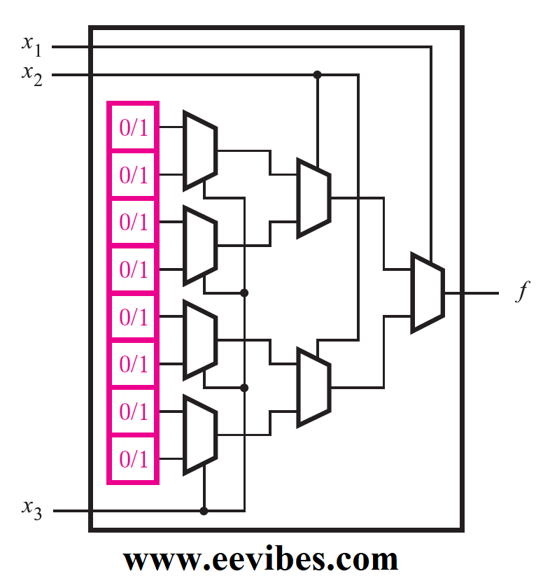
What is 3 input LUT?
Three-input LUT is shown in figure below. Because a three-variable truth table has eight rows, it has eight storage cells. LUTs often contain four or five inputs in commercial FPGA devices, requiring 16 or 32 storage cells, respectively. We saw in Figure 3.29 that PALs frequently contain additional circuitry with their AND-OR gates. The same is true for FPGAs, which often have additional circuitry in each logic block in addition to a LUT.
A flip-flop can be inserted in an FPGA logic block, as seen in Figure below.
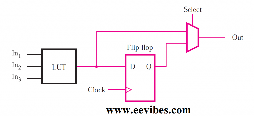
As already stated the flip-flop is used to hold the value of its D input under the control of its clock input, Each logic function in a logic circuit must be tiny enough to fit into a single logic block for it to be realized in an FPGA. In practice, utilizing CAD tools, a user’s circuit is automatically translated into the needed form . When a circuit is implemented in an FPGA, the logic blocks are programmed to perform the appropriate functions, and the routing channels are programmed to connect the logic blocks together. The ISP approach, is used to configure FPGAs. The storage cells of an FPGA’s LUTs are volatile, meaning they lose their stored contents if the chip’s power supply is switched off. As a result, every time power is applied, the FPGA must be programmed. A programmable read-only memory (PROM), a tiny memory chip that stores data permanently, is frequently inserted on the circuit board that houses the FPGA. When power is applied to the chips, the storage cells in the FPGA are immediately loaded from the PROM.
Following Figure shows a small FPGA that has been designed to implement a circuit. Each routing channel contains four wires and two input LUTs on the FPGA.
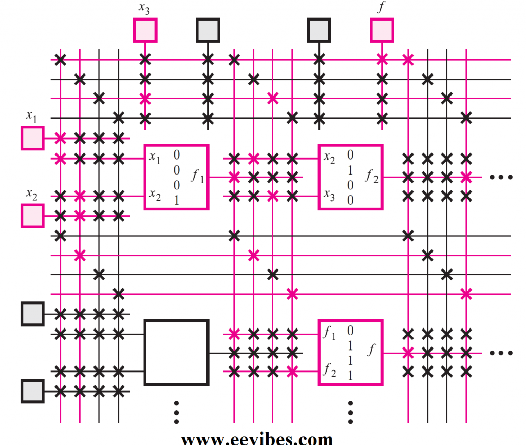
In this area of the FPGA, the programmed states of both the logic blocks and wiring switches are shown. An X indicates programmable wiring switches. Each of the blue switches is turned on, and a horizontal and vertical cable is connected.
The black switches have been switched off. The functions f1 = x1x2 and f2 = x2]x3 are represented by the truth tables programmed into the logic blocks on the top row of the FPGA. The logic block in the bottom right corner of the diagram is designed to create f = f1 + f2 = x1x2 +x2’x3.
Also read here
- What are the synchronous counters? Explain with an example.
- what are the half adder and full adder circuits?
- what are the half subtractor and full subtractor circuits?
- How to design a four bit adder-subtractor circuit?
- What are number systems in computer?
- Discuss the binary counter with parallel load? Explain its working with an example
- how to draw state diagram of sequential circuit?
- How to simplify a Boolean function using Karnaugh map (k-map)?
- What are the flip flops and registers in digital design?
- Define fan-in, fan-out, CMOS and TTL logic levels
- what is the Canonical form representation of Boolean function?
- What is difference between latches and flip flops?
- What are the Transistor Switches?
- What are the synchronous and asynchronous counters?
- What are the Parallel Access Shift Registers?
- What are the applications of decoder circuits?