Transistor Switches
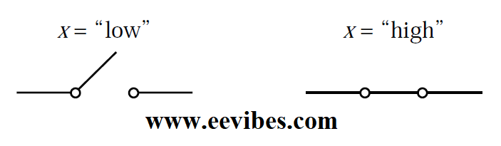
What are the Transistor Switches? Transistors are used in logic circuits. We can presume that a transistor is used to understand how logic circuits are created. It works as a simple switch. A switch controlled by a logic signal, x, is shown in figure below. When The switch is open when x is low, and closed when x is high. The most widely used type: The metal oxide semiconductor field-effect transistor is used to build a basic switch (MOSFET). MOSFETs are divided into two categories:
- n-channel and
- p-channel.
NMOS and PMOS stand for N-channel and P-channel, respectively.
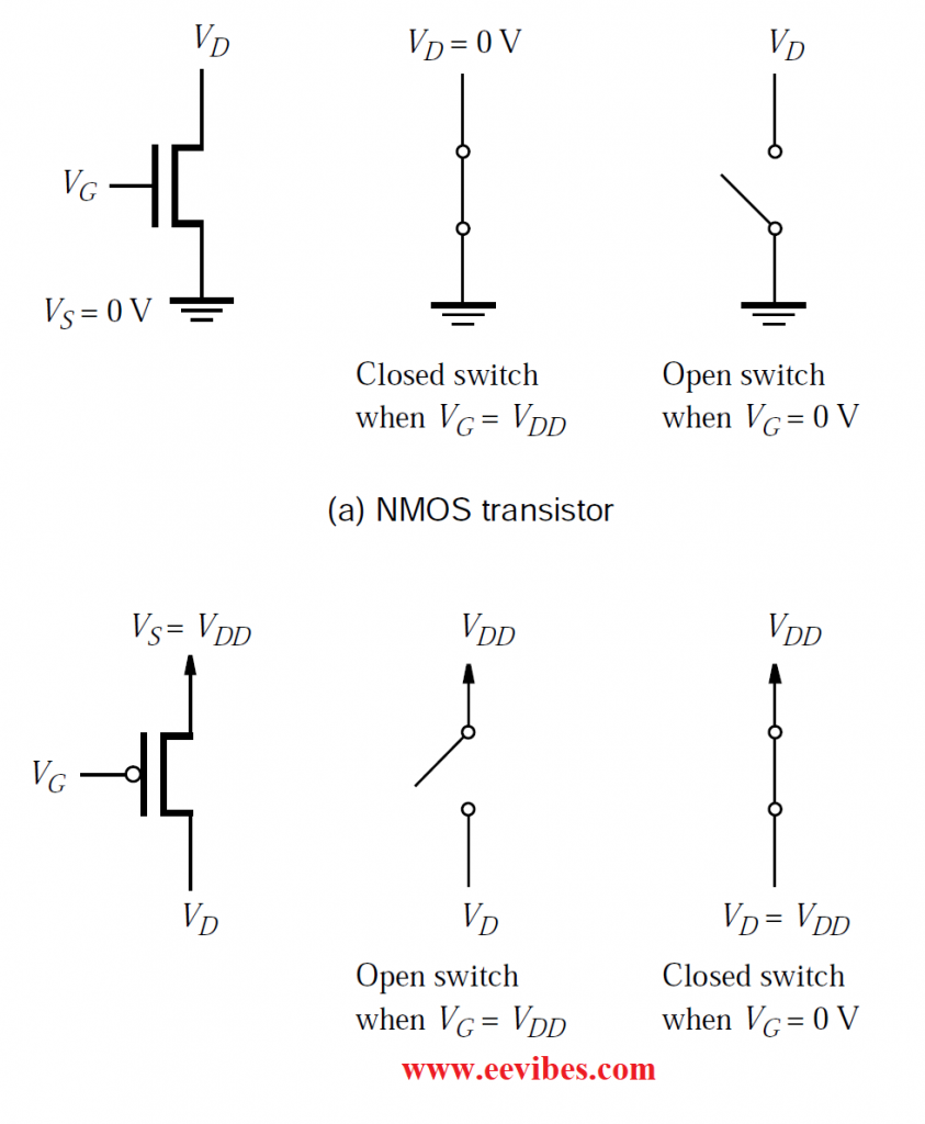
An NMOS transistor is depicted graphically in Figure below. The source, drain, gate, and substrate are the four electrical terminals. Ground (Gnd) is connected to the substrate (also known as body) terminal in logic circuits.
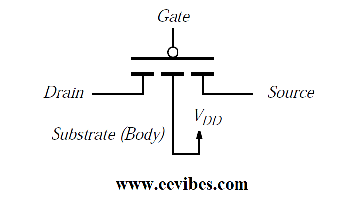
The source and drain terminals have no physical distinctions. In actuality, the voltage levels applied to the transistor distinguish them; by convention, the terminal with the lowest voltage level is considered the source.
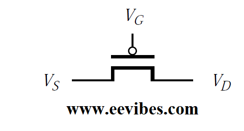
This transistor is controlled by the voltage VG at the gate terminal. If VG is low, the transistor is shut off since there is no connection between the source and drain. When VG is high, the transistor is activated and operates as a closed switch between the source and drain terminals. For the time being assume the resistance is zero.
PMOS transistors behave differently than NMOS transistors. The former are used to create the switch, in which the switch is open when the control input x is high and closed when x is low. above figure depicts a symbol.
The PMOS transistor’s substrate is always linked to VDD in logic circuits, resulting in the simplified symbol in Figure below. If VG is high, the PMOS transistor is turned off and operates like an open switch. The transistor is turned on and operates as a closed switch that connects the source and drain when VG is low. The source of a PMOS transistor is the node with the greater voltage.
Following figure shows how NMOS and PMOS transistors are commonly used in logic circuits. When the gate terminal of an NMOS transistor is high, it is turned on, and when the gate terminal of a PMOS transistor is low, it is turned on. The NMOS transistor’s drain is drawn down to Gnd when it is switched on, while the PMOS transistor’s drain is pulled up to VDD when it is turned on. An NMOS transistor cannot be utilized to draw its drain terminal completely up to VDD due to the way transistors work. Similarly, a PMOS transistor’s drain terminal cannot be pulled all the way down to Gnd.
What are the NMOS Logic Gates?
In the 1970s, the first schemes for building logic gates with MOSFETs became popular, although they only used PMOS or NMOS transistors, not both. A mix of NMOS and PMOS transistors has been employed since the early 1980s. We’ll start by going through how to make logic circuits with NMOS transistors because they’re easier to understand. NMOS circuits are the name for such circuits. Then we’ll illustrate how NMOS and PMOS transistors are merged in the complementary MOS, or CMOS, technology, which is currently quite common.
When Vx = 0 V in the circuit in figure below the NMOS transistor is turned off. The resistor R conducts no current, and Vf = 5 V. When Vx = 5 V, on the other hand, the transistor turns on and pulls Vf to a low voltage level. The amount of current flowing between the resistor and transistor determines the exact voltage level of Vf in this situation.
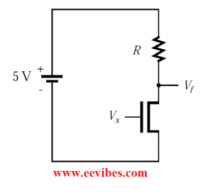
Vf is usually around 0.2 V. The circuit is an NMOS implementation of a NOT gate if Vf is seen as a function of Vx. This circuit implements the function f = x in logic terms. Following Figure shows a simplified circuit schematic with an arrow labelled VDD indicating the connection to the positive power supply terminal and the Gnd symbol indicating the connection to the negative power supply terminal.
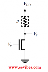
When Vx = 5 V, the resistor in the NOT gate circuit serves to limit the amount of current flowing. A transistor is usually used instead of a resistor for this reason. A dashed box is added around the resistor R in subsequent diagrams as a reminder that it is accomplished using a transistor.
The graphical symbols for a NOT gate are shown in Figure below.
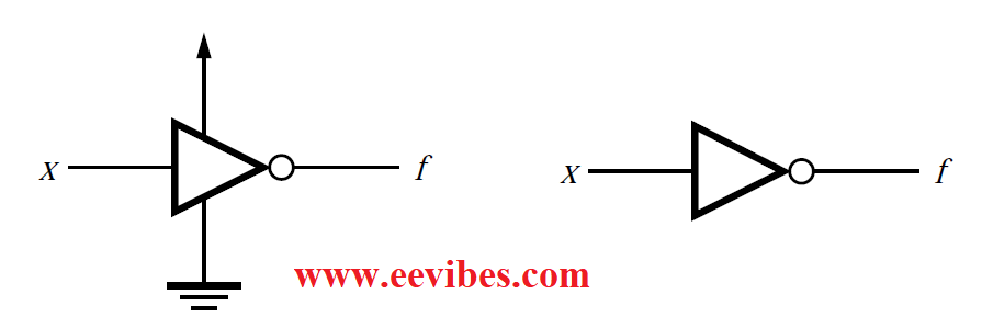
The input, output, power, and ground terminals are shown on the left symbol, while the input and output terminals are only shown on the right symbol. Only the simplified sign is used in practice. The inverter is another name for the NOT gate. In this book, we use both names interchangeably.
The logic AND function is represented by a series connection of switches, whereas the OR function is represented by a parallel connection.
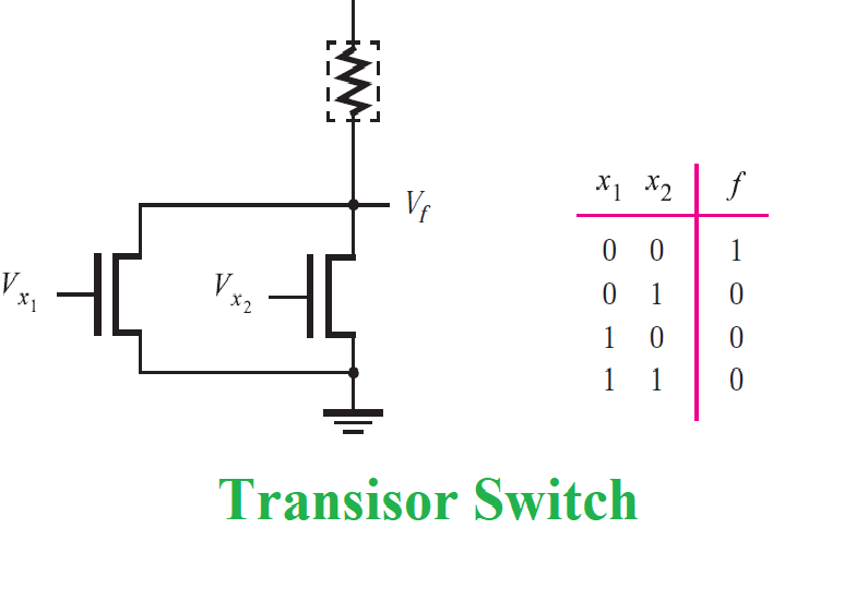
We can create the series connection shown in Figure below using NMOS transistors. Both transistors will be on if Vx1 = Vx2 = 5 V, and Vf will be close to 0 V. When either Vx1 or Vx2 is 0, no current flows through the series-connected transistors, and Vf is brought up to 5 V.
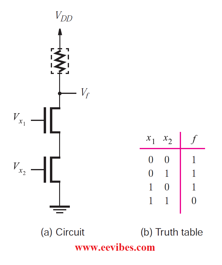
Above Figure shows the truth table for f, which is given in terms of logic values. The realized function is the NOT-AND complement of the AND function, known as the NAND function. A NAND gate is implemented in the circuit. Figure 3.6c depicts its graphical symbols.
Figure below shows the parallel connection of NMOS transistors. If either Vx1 or Vx2 are both 5 V, then Vf will be close to 0 V. Vf will only be brought up to 5 V if both Vx1 and Vx2 are 0.
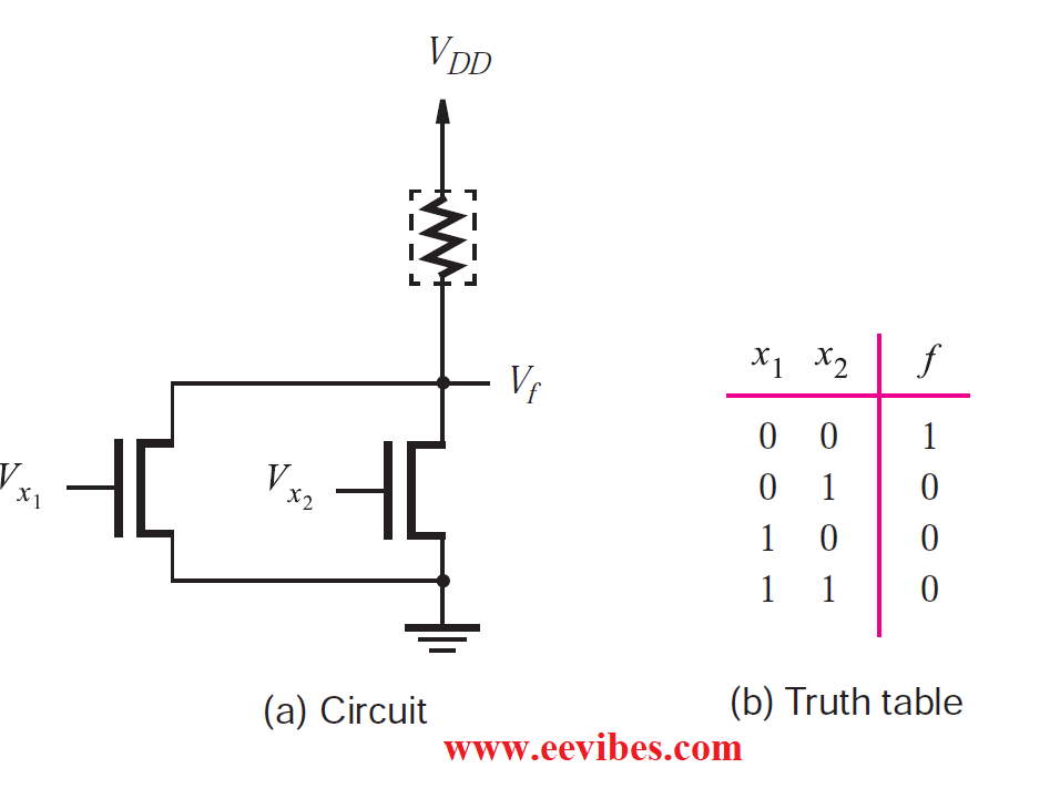
Figure below shows a related truth table. It demonstrates that the circuit achieves the NOR function, which is the complement of the OR function.
The reader would naturally be interested in the AND and OR gates that were used extensively in the previous chapter, in addition to the NAND and NOR gates just discussed.
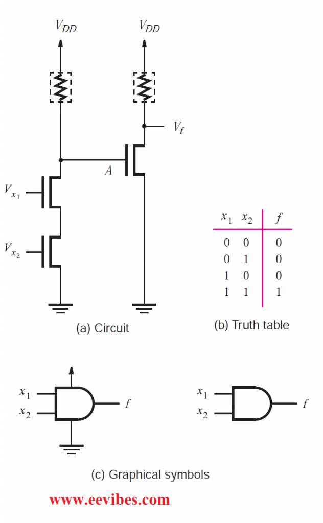
In NMOS technology, an AND gate is formed by following a NAND gate with an inverter, as shown in Figure below. The NAND of inputs x1 and x2 is realized by Node A, and the AND function is represented by f. An OR gate is also implemented as a NOR gate followed by an inverter.
Related Topics
- What are the synchronous counters? Explain with an example.
- what are the half adder and full adder circuits?
- what are the half subtractor and full subtractor circuits?
- How to design a four bit adder-subtractor circuit?
- What are number systems in computer?
- Discuss the binary counter with parallel load? Explain its working with an example
- how to draw state diagram of sequential circuit?
- How to simplify a Boolean function using Karnaugh map (k-map)?
- What are the flip flops and registers in digital design?
- Define fan-in, fan-out, CMOS and TTL logic levels
- what is the Canonical form representation of Boolean function?
- What is difference between latches and flip flops?