Dynamic Operation of Logic Gates
Discuss the Dynamic Operation of Logic Gates. Logic gates are devices which are idealized as physical devices to digital circuits. This logic circuit performs the basic logic functions that form the basis of digital circuits. Logic gates are used in the devices we use nowadays such as computers and memory devices. Circuit logic gates make decisions based on a set of digital signals that come from their inputs.
Many of the logic gates have two inputs and one output. Logic gates are based on Boolean algebra. Each step is either in the false or true state of the two binary options. False represents 0, while true represents 1. Depending on the type of logic gates or inputs used , the binary output will change accordingly . The output of the logic gate is 0 in one position and 1 in the other position similar to the light switch. They can be termed as integrated circuits.
Combinations of these logic gates can perform many operations. The total number of gates that can be arranged in an array and used in one device is theoretically unlimited. The number of gates that can truly fit into a given physical location is limited. In digital integrated circuits, there are arrays of logic gates.
AND Gate
The AND gate is known, so if 0 is called ‘false’ and 1 is called ‘true’, then the gate works the similar way as the logical ‘and’ operator.
OR Gate
The output is “true” on the OR gate if one or both inputs are “true”. If both inputs are “false”, the output is “false”. In other words, for having the output to be 1, the input must be at least one or two 1s.
XOR Gate
An XOR (exclusive OR) gate is identical to an “either/or” gate. The output is “true” if either input, but not both, is “true”. The output is “false” if both inputs are “false” or if both inputs are “true”. In other words, the output is 1 if the inputs are different, but 0 if the inputs are the same.
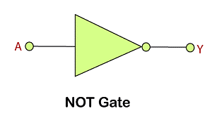
NOT Gate
The logic inverter, sometimes called a NOT gate to distinguish it from other types of electronic inverter devices, has a single input. Reflects the logical state. If the input is 1, the output is 0. If the input is 0, the output is 1.
NAND Gate
The NAND gate acts as an AND gate followed by a NOT gate. It behaves in the manner of the logical process ‘and’ followed by negation. The output is “false” if both inputs are “true”. Otherwise, the output is True.
NOR Gate
A NOR gate is a composite OR gate followed by an inverter. Its output is “true” if both inputs are “false”. Otherwise, the output is true.
XNOR Gate
An XNOR (Exclusive-NOR) gate is a composite XOR gate followed by an inverter. Its output is “true” if the inputs are the same and “false” if the inputs are different.
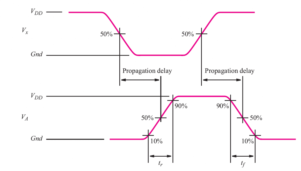
The Node between the two gates is labeled A because it is distributing the capacitive load to both. Two types of material overlapped between them. The presence of stray capacitance has a negative effect on the running speed logic circuits.
The voltage across the capacitor cannot change instantly. Time for the charge or discharge of the capacitor depends on the size of the capacitance C and the quantity of the current through the capacitor. When the PMOS transistor is in N1 is turned on, the capacitor is charged to VDD; It is discharged at the NMOS transistor running.
In each case, the identifier of the current flowing through the embedding transistor and the value from C determines the rate of charge and discharge of the capacitor.
This equation tells us the speed of the circuit depends upon both the values. The expression show the time of propagation when the output changes from high level to low level. The low to high level is also given by the above equation .In logic gates we usually set the value of L to minimum level for the specification required. The value of W is chosen according to the amount of current flow
There is a particular method involved in choosing transistors sizes because a larger transistor takes more space on the chip rather than the other one. The proportionality of C to the W and L tends to improve the expected performance. They are utilized where high capacitive loads must be driven and and signal propagation must be delayed accordingly.
Also read here
- What Types of CAD Tools are Used for Designing a Digital System?
- What happens when you apply asynchronous inputs to flip flops?
- How to design a 4 bit magnitude comparator circuit? Explanation with examples
- What is the magnitude comparator circuit? Design a 3 bit magnitude comparator circuit
- What are the synchronous counters? Explain with an example.
- what are the half adder and full adder circuits?
- what are the half subtractor and full subtractor circuits?
- How to design a four bit adder-subtractor circuit?
- What are number systems in computer?
- Discuss the binary counter with parallel load? Explain its working with an example
- how to draw state diagram of sequential circuit?
- How to simplify a Boolean function using Karnaugh map (k-map)?
- What are the flip flops and registers in digital design?
- Define fan-in, fan-out, CMOS and TTL logic levels
- what is the Canonical form representation of Boolean function?
- What is difference between latches and flip flops?