Introduction
What are the Practical Aspects of Digital Circuit Design? The practical aspects of digital circuit design describe how transistors are embedded in silicon and matters related to their operations. Additionally, it concerns the reliability of logic circuits as well as significant challenges with signal propagation delays and power consumption in logic gates.
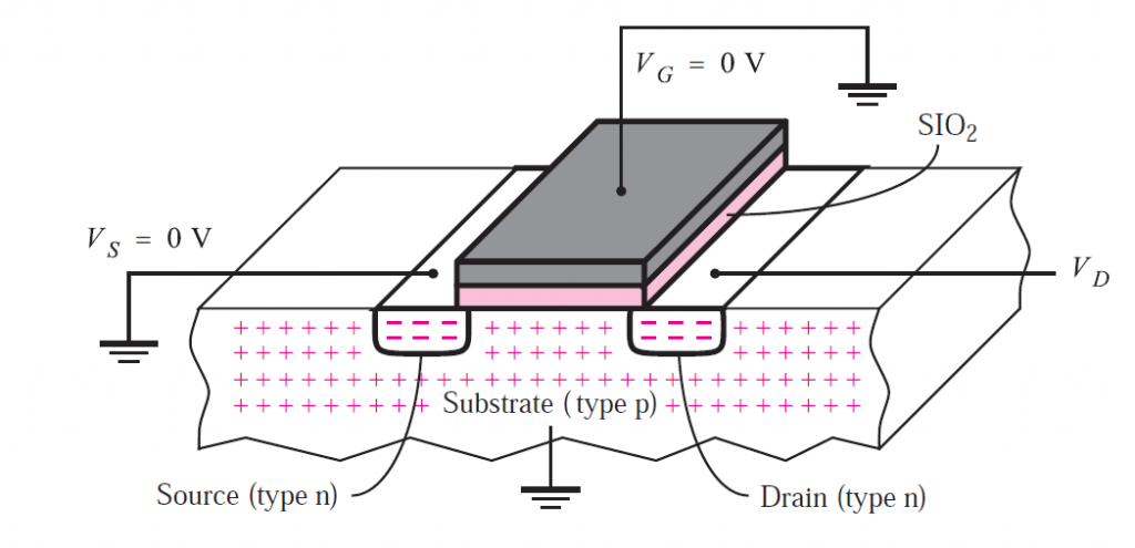
MOSFET Fabrications and Behavior
The gate terminal was constructed of metal when MOSFETs were first developed. Now, a substance called polysilicon is utilized. Although polysilicon is a conductor, unlike metal, it is preferred because it possesses characteristics that make it possible to construct MOSFETs with incredibly tiny dimensions. A layer of silicon dioxide (SiO2) serves as an electrical insulator between the gate terminal and the transistor substrate. It also acts as an insulator between the gate electrically from the remainder of the transistor. Electrical fields generated by voltages supplied to the transistor’s terminals control how it operates.
Consider the first case when the source and gate are both connected to Ground. The p-type substrate separates the n-type source and n-type drain from one another. There are two diodes between the source and drain in an electrical circuit. One diode is formed by the p-n junction between the substrate and source, while the other one is formed by the p-n junction between the substrate and drain.
These back-to-back diodes depict an extremely high resistance that restricts current passage between the drain and source. In this condition, we refer to the transistor as being shut off or turned off. The impact of raising the voltage at the gate terminal in relation to the voltage at the source is the next thing to examine.
The gate-to-source voltage is represented as VGS. The transistor converts from being an open switch to a closed switch if VGS is larger than a specific minimum positive value known as the threshold voltage VT, as discussed below. Although several factors affect the precise degree of VT, it is normally around 0.2 VDD.
The PMOS Transistor
Except for the fact that all voltages and currents are reversed, PMOS transistors behave exactly like NMOS transistors. The PMOS transistor’s source terminal has a greater voltage level than the other terminals, and a negative threshold voltage is needed to turn the transistor on. The physical structure of PMOS transistors is identical to that of NMOS transistors, with the exception that type p silicon is used in place of type n silicon in the PMOS transistor and vice versa. Connecting the source and gate nodes of a PMOS transistor to VDD turns the transistor off. We would put the gate node to Ground to switch on the PMOS transistor, resulting in VGS = 5 V.
Noise Margins
Noise, which is a persistent source of random disturbances in electronic circuits, can change the output voltage levels generated by the gate N1. The gate N2 must not perceive a low logic value as a high one or vice versa as a result of this noise. Consider the scenario when N1 generates its low voltage level VOL. Noise may change the voltage level, but if it stays below VIL, N2 will still perceive it appropriately.
The ability to tolerate noise without affecting the correct operation of the circuit is known as noise margin. For the low output voltage, we define the low noise margin as
NML = VIL – VOL
The scenario is identical when N1 generates its high output voltage VOH. Any circuit noise may change the voltage level, but if the voltage is higher than VIH, N2 will read it appropriately. The high noise margin is defined as
NMH = VOH – VIH
Fan-in in Logic Gates
Fan-in is a term that characterizes the most extreme number of computerized inputs that a solitary rationale entryway can acknowledge. Most semiconductor transistor (TTL) entryways have a couple of data sources, albeit some have more than two. A normal rationale entryway has a fan-in of 1 or 2. 1 happens to be only in NOT gate.
In some advanced frameworks, it is important for a solitary TTL rationale entryway to drive a few gadgets with fan-in numbers more noteworthy than 1. Whenever, in a Transistor-to-Transistor Logic the number of inputs that must be driven exceeds the value of 10, Buffer if used. It is placed between the gate output of TTL and inputs of the device. An intelligent inverter (additionally called a NOT entryway) can serve this capacity in most computerized circuits.
What is the difference between fan-in and fan-out? Examples
Fan-out in Logic Gates
The fan-out is characterized as the most extreme number of inputs that can be associated with the output of a logic gate without debasing the typical operation. Fan Out is determined from the measure of current accessible in the yield of an entryway and the measure of current required in each input of the associating logic gate. It is determined by manufacturers and is given in the information sheet. Surpassing the predefined greatest burden might cause a glitch on the grounds that the circuit won’t be capable inventory the requested force.
The contrast between these two qualities of a computerized IC is huge from the definitions above.
Buffers
Buffers are frequently employed in circuits when a logic gate must drive a sizable capacitive load to enhance performance. A buffer is a logic gate that has one input “a”, one output “b”, and delivers the result that a = b. Depending on the size of the transistors, buffers may be made with varying drive capacities. Buffers often feature transistors that are bigger than those in regular logic gates since they are used to drive higher-than-normal capacitive loads. The inverting buffer is a different kind of buffer. It uses relatively big transistors yet generates the same output as an inverter. It can drive huge capacitive loads and has the same graphical representation as a NOT gate.
Also read here
- What are the CMOS Logic Gates?
- How to design a 4 bit magnitude comparator circuit? Explanation with examples
- What is the magnitude comparator circuit? Design a 3 bit magnitude comparator circuit
- What are the synchronous counters? Explain with an example.
- How to design a 4 bit magnitude comparator circuit?
- what are the half adder and full adder circuits?
- what are the half subtractor and full subtractor circuits?
- How to design a four bit adder-subtractor circuit?
- What are number systems in computer?
- Discuss the binary counter with parallel load? Explain its working with an example
- how to draw state diagram of sequential circuit?
- How to simplify a Boolean function using Karnaugh map (k-map)?
- What are the flip flops and registers in digital design?
- Define fan-in, fan-out, CMOS and TTL logic levels
- what is the Canonical form representation of Boolean function?
- What is difference between latches and flip flops?