Shift and add multiplier circuit
Shift-and-add multiplication method adds the multiplicand X to itself Y times, where Y is the multiplier. What are the Shift and Add Multiplier Circuits?
Multiplier circuit:
A multiplier is basically a combinational logic circuit which we use in multiplication of binary digits. Similar to the adder and subtractor, a multiplier is an arithmetic combinational logic circuit. It is called as binary multiplier or digital multiplier.
How shifts are multiplied?
For multiplication of a number, a binary shift moves all the digits in the binary number along to the left and by filling the gaps after the shift with 0
For multiplying by two, all digits shift one place to the left.
Building multipliers
A multiplier is an electronic circuit that is used to multiply two binary numbers. Assembled utilizing parallel adders that are full adders.. It’s used to eliminate the least significant bits of the product.
What is multiplier and accumulator?
In computing, the multiply–accumulate (MAC) or multiply-add (MAD) operation is a common step that computes the product of two numbers and adds that product to an accumulator.
Explanation
A circuit in which two unsigned n-bit binary numbers are multiplied. The circuit contains a two-dimensional array of similar sub circuits in which each one contains a full-adder and an AND gate.
If large values of n are present, this procedure is not considerable as the large number of gates would be needed. To use different approach, we use a shift register with an adder in implementation of classical method of multiplication.
The manual process of multiplying two binary numbers is done by the product that is formed by a series of addition operations done. For every bit “i” in the multiplier considered is 1, the value of the multiplicand shifted to the left “i” times is added to the product.
A pseudo code is presented where A is the multiplicand, B is the multiplier and P is product.
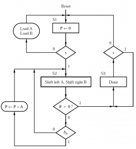
An ASM chart is presented in which the assumption is that an input “s” is used when the machine initializes the multiplication process.
The longest “s” is 0, the machine remains in the state S1 and from external inputs, the data for A and B can be loaded.
In state S2 we observe the value of the least significant bit of B, and if it is 1, we’ll add A to P. Otherwise, P will not be changed.
In state S3, when B is 0, and P has the final product.
For every clock cycle when machine is in state S2, we’ll shift the value in A to the left according to the pseudo-code. The contents of B are shifted to the right because in each clock cycle b=0 can be used in deciding whether A should be added to P or not.
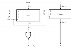
Data path Circuit
To implement A, a right-to-left shift register is used that has 2n bits. A 2n-bit register is required for P, and it should include an enable input because the assignment P ← P + A in state S2 is inside a conditional output box. A 2n-bit adder is required to produce P + A.
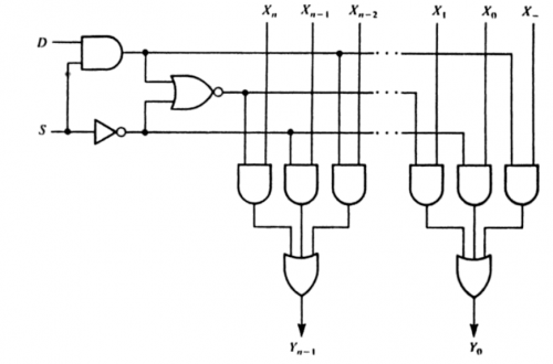
Considered that P is loaded with 0 in state S1, and P is loaded from the output of the adder in state S2. One can’t assume that the reset input is used to clear P, because the machine changes from state S3 back to S1 based on the s input, not the reset input. Hence a 2-to-1 multiplexer is needed for each input to P, to select either zero or the appropriate sum bit from the adder. An n-bit left-to-right shift register is needed for B, and an n-input NOR gate can be used to observe whether B = 0.
Control signals can be labelled for the shift registers. The input data for the shift register is named as Data A. The shift register having 2n bits, the main n data inputs are connected with 0. A solo multiplexer symbol is shown connected with the register that holds P. This sign addresses 2n 2-to-1 multiplexers that are each constrained by the Psel signal.
Control Circuit
An ASM chart requires control signals for the multiplier. In state S1, Psel will be set to 0 and EP is affirmed, so that register P is cleared. When s = 0, parallel data can be loaded into shift registers A and B by an external circuit that will controls their parallel load inputs LA and LB.
When s = 1, the machine changes its state to S2, where Psel is set to 1 and shifting of A and B will be enabled. In the event if b0 = 1, enable for P is asserted. The machine changes to state S3 when z = 1, and afterward stays in S3 and sets Done to the value 1 until s = 1.
VHDL Code
In this the number of bits in A and B will be set by the generic parameter N. Since some registers are 2n bits wide, a second generic parameter NN is defined which will represent 2×N. By changing the value of the generic parameters, the code can be used for numbers of any size.
In the control circuit, processes labelled FSM transitions and FSM outputs define the state transitions and generated outputs, respectively. The parallel data input on the shift register A is 2N bits wide, but Data A is only N bits wide.
The signal N Zeros is used to generate n zero bits, and the signal A in prepends these bits with Data A for loading into the shift register. A FOR GENERATE statement is required in which the multiplexer needed for register P is defined using that instantiates 2N 2-to-1 multiplexers.
A simulation resulted for the circuit is generated from the code. After the circuit is reset, LA and LB are set to 1, and the numbers to be multiplied are placed in the Data A and Data B inputs. After s is set to 1, the FSM will be converted to state S2, where it remains until B = 0. For each clock cycle in state S2, A is moved to the left, and B is moved to the right. In three of the clock cycles in state S2, the contents of A are added to P, corresponding to the three bits in B that have the value 1.
When B = 0, the FSM changes to state S3 and P contains the correct product, which is
〖(64)〗_16 × 〖(19)〗_16 =〖(9C4)〗_16
The decimal equivalent of this is 100 × 25 = 2500. The number of clock cycles required for the circuit is generated by the final product which is determined by the left-most digit in B that is 1. It is possible to decrease the number of clock cycles required by using more intricate shift registers for A and B. If the two right-most bits in B are both zero, then both A and B could be shifted by two bit positions in one clock cycle. Similarly, if the three lowest digits in B are 0, then a three bit-position shift can be done, and it will continue. A barrel shifter is used in shift register for shifting multiple bit positions at once.
Also read here:
- How to Design Counters Using Sequential Circuits?
- What are the CMOS Logic Gates?
- What is the magnitude comparator circuit? Design a 3 bit magnitude comparator circuit
- What are the synchronous counters? Explain with an example.
- what are the half adder and full adder circuits?
- what are the half subtractor and full subtractor circuits?
- How to design a four bit adder-subtractor circuit?
- What are number systems in computer?
- Discuss the binary counter with parallel load? Explain its working with an example
- how to draw state diagram of sequential circuit?
- How to simplify a Boolean function using Karnaugh map (k-map)?
- What are the flip flops and registers in digital design?
- Define fan-in, fan-out, CMOS and TTL logic levels
- what is the Canonical form representation of Boolean function?
- What is difference between latches and flip flops?