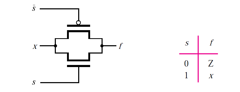
Transmission Gates
What are the Transmission Gates? A transmission gate, or analog switch, is defined as an electronic element that will selectively block or pass a signal level from the input to the output.”
This solid-state switch is comprised of a PMOS transistor and NMOS transistor. The control gates are biased in a complementary manner so that both transistors are either ON or OFF.
Basic Operation
When the voltage on node A is a Logic 1, the complementary Logic 0 is applied to node active-low A, allowing both transistors to conduct and pass the signal at IN to OUT. When the voltage on node active-low A is a Logic 0, the complementary Logic 1 is applied to node A, turning both transistors off and forcing a high-impedance condition on both the IN and OUT nodes. This high-impedance condition represents the third “State” (high, low, or high-impedance(Z)) that the channel may reflect downstream.
The schematic diagram includes the arbitrary labels for IN and OUT, as the circuit will operate in an identical manner, if those labels were reversed. This design provides true bidirectional connectivity without degradation of the input signal.
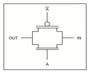
CMOS Transmission Gate or Pass Gate
- “The CMOS transmission gate consists of one NMOS and one PMOS transistor, connected in parallel.”
- The gate voltages applied to those two transistors are also set to be complementary signals.
- Thus, the CMOS Transistor Gate operates as a bidirectional switch between the nodes A and B which is controlled by signal C.
- If the control signal C is:
- Logic-High, that is equal to VDD, then both transistors are turned on and provide a low-resistance current path between the nodes A and B.
- Low, then both transistors will be off, and the path between the nodes A and B will be an open circuit. This condition is also called the high-impedance state.
- The NMOS switch passes a good zero but a poor 1.
- The PMOS switch passes a good 1 but a poor 0.
- Transmission Gates are efficient in implementing some functions such as multiplexers, XORs, XNORs, latches, and Flip-Flops.
- For a detailed DC analysis of the CMOS transmission gate, we will consider the following bias condition:
- The input node(A) – constant logic-high voltage, Vin = VDD.
- The control signal (C) – logic-high (ensuring that both transistors are turned on).
- The output node (B) – connected to a capacitor (capacitive loading of the subsequent logic stages driven by the transmission gate).
Working of Transmission Gates
- Let’s suppose that, this is our Transmission Gate.
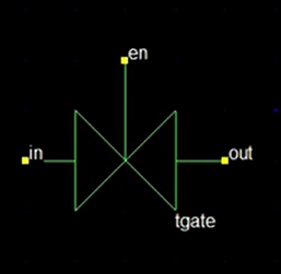
- Complete the circuit and label the input and output.
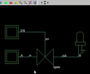
- When we run the circuit in simulator, output point B is in High-Impedance state(Z).
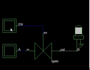
- Whether we turn ON or OFF the Input point A, output point B is still in High-Impedance state (Z). The reason behind this is that the Enable point EN is turned off.

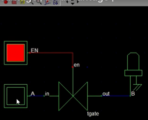
- When we turn ON the EN point regardless the input point A, the output point B will be zero (LED will be turned off).

- When we turn ON EN point, and turn OFF input A, then output B will be zero or OFF.
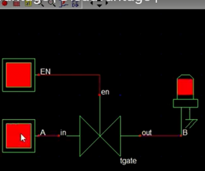
- When we turn ON EN point, and turn ON input point A, then output point B will be One or ON.
ADVANTAGES
- There is no degradation in the output logic level.
- It is more sensitive.
- Less propagation Delay.
DISADVANTAGES
- Required both NMOS and PMOS in different wells.
- Both true and complemented polarities of the control signal needed.
- Parallel connection of both transistors increases node capacitance.
Also read here
- What are the Techniques for Testing Digital Circuits?
- How to Design Counters Using Sequential Circuits?
- What are the CMOS Logic Gates?
- What is the magnitude comparator circuit? Design a 3 bit magnitude comparator circuit
- What are the synchronous counters? Explain with an example.
- what are the half adder and full adder circuits?
- what are the half subtractor and full subtractor circuits?
- How to design a four bit adder-subtractor circuit?
- What are number systems in computer?
- Discuss the binary counter with parallel load? Explain its working with an example
- how to draw state diagram of sequential circuit?
- How to simplify a Boolean function using Karnaugh map (k-map)?
- What are the flip flops and registers in digital design?
- Define fan-in, fan-out, CMOS and TTL logic levels
- what is the Canonical form representation of Boolean function?
- What is difference between latches and flip flops?