Introduction to Arbiter
Explain the FSM as an Arbiter Circuit in Details? The purpose of machine is to control access by many devices to a shared resources in a given system. Only one device can use the source at a time. Assume that all signals in the system can change values only on the positive verge of the clock signal. Each device provides one input to the FSM, called a request, and the FSM produces a separate output for each device, called a grant. A device shows its need to use the resource by asserting its request signal. Whenever the shared resource is not already in use, the FSM considers all requests that are active. It chooses one of the seeking devices based on a priority mechanism and assert its grant signal. When the product is complete if these devices is completed operating the resource, it de-asserts its demand signals.
We will assume that there are three devices in the system called device 1, device 2, and device 3. It is easy to see how the FSM can be extended to handle more devices. The request signals are named r1, r2, and r3, and the grant signals are known as g1, g2 and g3. The devices are assigned important levels such that device 1 has got the greatest priority, device 2 has got the next highest and device 3 has the lowest priority. Thus if more than one request transmission is asserted when the FSM assigns a grant, the grant is given to the requesting device that has the highest priority.
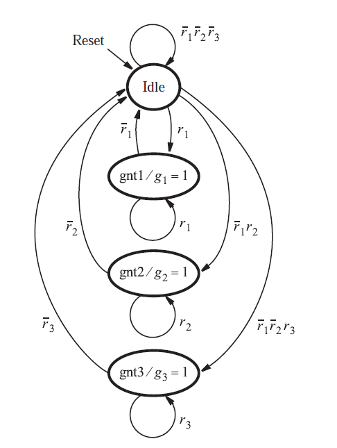
A state diagram for the desired FSM, designed as a Moore-type machine, is shown in Figure 1. In the beginning, on reset the machine is in the state called Idle. No grant signals are declared, and the shared resource is not being used. There are three other states, called gnt1, gnt2, and gnt3. Each of these states asserts the grant signal for one of the devices.
The FSM stays in the Idle state as long as all of the request signals are 0. In the state diagram the condition r1r2r3 = 000 is indicated by the arc labelled 000. When one or more request signals become 1, the machine moves to one of the grant states, with respect to the priority scheme. If r1 is asserted, then device 1 will receive the grant because it has the highest priority. This is indicated by the arc labelled 1xx that leads to state gnt1, which sets g1 = 1. The meaning of 1xx is that the request signal r1 is 1, and the values of signals r2 and r3 are irrelevant because of the priority scheme. As before, we use the symbol x to indicate that the value of the corresponding variable can be either 0 or 1. The machine stays in state gnt1 as long as r1 is 1. When r1 = 0, the arc labelled 0xx causes a change on the next positive clock edge back to state Idle, and g1 is de-asserted. If other requirements are active at this time, then the FSM will change to a new contribution state after the next clock edge.
The gnt2 state is changed by the arc with the designation 01x. Because it depicts the circumstances where r2 = 1, but r1 =0, this label complies with the priority system. Similarly, the prerequisite for entering state gnt3 is specified as 001, meaning that r3 is the only asserted request signal means demanding signals.
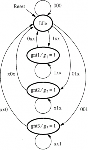
The state diagram is repeated in Figure 2. The only difference between this diagram and Figure 1 is the way in which the arcs are categorized. Figure 2 uses a simpler labelling scheme that is more intuitive. For the condition that leads from state Idle to state gnt1, the arc is labelled as r1, instead of 1xx. This mark is actually means that if r1 = 1, the FSM changes to state gnt1, regardless of the other inputs. The arc with the label r1r2 that leads from state Idle to gnt2 represents the condition r1r2 = 01, while the value of r3 is irrelevant. There is no standardized scheme for classification of the arcs in state diagrams. Some inventors prefer the style of Figure 1, while others prefer a style more similar to Figure 2.
The VHDL code for the Arbiter
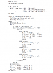
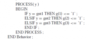
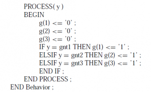
Three-bit STD LOGIC VECTOR signals are used to specify the three request and grants signals. The CASE statement used for the figure 8.29 is used to explain the FSM. It is simple to express the necessary priority scheme, as explained in the WHEN clause for state Idle. The IF statement states that the machine will enter the gnt1 state if r1 = 1. The ELSIF condition, which specifies that if r2=1, the next state will be gnt2, is examined if r1 is not asserted. Only if none of the higher priority request signals are proclaimed does each subsequent ELSIF clause take a lower-priority request signal into account.
The WHEN clause for each grant state is straightforward (direct). For state gnt1 is specifies that as long as r1 = 1, the next state remains gnt1. When r1=0, the next state is idle. The other grant states have the same structure.
The code for the grant signals, g1, g2, and g3 is given at the end. It sets g1 to 1 when the machine is in state gnt1 and otherwise g1 is set to 0. Correspondingly, each of the other grant signals is 1 only in the appropriate grant state.
VHDL code for the arbiter
Implementation of the Arbiter Circuit
Now we will consider the effects of implementing the arbiter in both a CPLD and an FPGA. Any differences between the two implementations are possible to be more prominent if the complexity of the FSM is greater. Hence instead of directly using the code in figure 3, we will implement a larger version of the arbiter that controls eight devices. The request signals are called r1, r2,…., r8, and the grant signals are g1, g2, ,…, g8. It is easy to see how the code in figure is extended to allow eight requesting devices, so we will not show it here,
Implementation in a CPLD
We first consider implementation of the arbiter in a CPLD. To represent the nine states in the FSM, the synthesis tool uses four flip-flops, called y4, y3, y2, andy1. The reset state idle is assigned the code y4y3y2y1y =0000. The other states are encoded as gnt1 = 0001,
gnt2 = 0010, gnt3 = 0100, gnt4 = 1000, gnt5 = 0011, gnt6 = 0101, gnt7 = 0110, and
gnt8 = 1001.
It is not obvious why the synthesis tool selected this specific state assignment. The tool considers many different state assignments and select one that minimizes the cost of the final circuit. For the CPLD implementation the synthesis tool attempts to choose the state assignment that results in the fewest product terms in the final circuit.
To see the complexity of the circuit, we need to observe the logic expressions generated for both the grant signals and the inputs to the state flip-flops. The expression for each grant signals is a direct result of the encoding used for the state that produces the grant. For case in point, state gnt8 is encoded as 1001, resulting in g8 = y4y3y2y1.
The logic feeding the state flip-flops is more complex. For example, the expression derived by the tool for the input Y4, to flip-flop y4 is
Y4 = r1r2r3r5r6r7r8y1y2y3y4 + r1r2r3r4y1y2y3 + r8y1y2y3y4 + r4y1y2y3y4
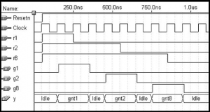
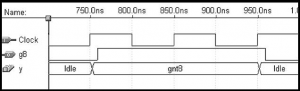
Figure above gives a timing stimulation for the CPLD implementation. For simplicity only the request signals r1, r2, and r8 are displayed along with the grant signals g1, g2, and g8. After the machine is reset at the beginning of the stimulation, all of the other request signals are set to 0. The machine first changes to the state gnt1 and asserts g1. After r1 becomes 0 the machine changes back to state-Idle. On the next clock cycle a transition to state gnt1 take place and g2 is asserted. After r2 becomes 0 the machine changes back to state idle, and then to state gnt8 to assert g8. The stimulation results indicate that the required priority scheme is properly implemented by our VHDL code.
Implementation in an FPGA
Next we study the implementing of the arbiter FSM in an FPGA chip. Instead of using four flip-flops to represent the nine states in the FSM, the FPGA implementation generated by the synthesis tool has nine state flip-flops called y9,y8,,….,y1. The state assignment is idle =00000000, gnt1 = 110000000, gnt2 = 101000000, gnt3 = 100100000, gnt4 =100010000, gnt5 = 100001000, gnt6 = 100000100, gnt7 = 100000010, and gnt8 =100000001. This assignment is very similar to the one hot encoding. The only difference is that the left most flip flop output y9, is complemented. This is done to provide a simple reset mechanism. When all flip-flops are reset, they define the state characterized variables being 0, which is the idle state.
Summary
Our arbiter FSM is a practical circuit that is useful in many types of system. For example; a computer in which various devices in the system are associated by a bus. One aspect of the arbiter may have to be changed for use in such a system. Because of the priority scheme, it is possible that devices with highly priority could prevent a lower-priority device from receiving a grant signal for an arbitrarily long time. This condition is frequently called starvation of the low priority device. It is mot difficulty to modify the arbiter FSM to justification for this issue.
Also read here
- What are the Techniques for Testing Digital Circuits?
- What are Arithmetic Comparison Circuits? Explain with examples.
- How to Design Combinational Logic Circuits by using Metaheuristic Algorithm?
- What are the Transmission Gates?
- What are number systems in computer?
- Number System Conversions – Briefly Explained
- How to design Half adder and Full adder circuits?
- What are the decoders? how are they different from encoders?
- What is binary arithmetic? How to add, subtract, multiply and divide two binary numbers?
- What is the magnitude comparator circuit? Design a 3 bit magnitude comparator circuit
- How to design a 4 bit magnitude comparator circuit?
- How many hundreds are there in 1000?
- What are the synchronous counters? Explain with an example
- what are the BCD and binary ripple counters?