
Parity Generator Circuit
How to Design an Even Parity or an Odd Parity Generator and Detector Circuit? A parity bit is used for error detection and correction in the communication and digital systems. So parity bit plays an important role while transmitting or receiving the binary information.
It is actually an extra bit that is added to the original message just to make the number of 1’s present in it either even or odd. This parity bit is then transmitted with the original message for detecting the errors. On the receiving side, the receiver uses this parity bit along with the original message to check there is some error or not.
If the checked parity is not similar to the transmitted parity, then an error is detected. The parity generator circuit is used for generating the parity bit. Similarly, a parity detector circuit is used for detecting the error.
Example of Even Parity Generator Circuit
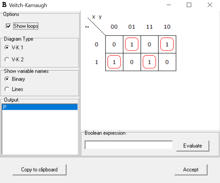
Consider we want to transmit a 3-bit message (xyz) that will be transmitted using even parity concept. The truth table for even parity generator is shown below:
| x | y | z | P |
| 0 | 0 | 0 | 0 |
| 0 | 0 | 1 | 1 |
| 0 | 1 | 0 | 1 |
| 0 | 1 | 1 | 0 |
| 1 | 0 | 0 | 1 |
| 1 | 0 | 1 | 0 |
| 1 | 1 | 0 | 0 |
| 1 | 1 | 1 | 1 |
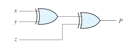
If you look carefully at the behavior of parity bit you can conclude that it can be implemented using the 3-input XOR gate function. Since XOR gate is an odd function. An odd function is a function which produces an output equal to 1 when there are odd number of 1’s in the input combination. So, the parity function can be implemented as:
P=x ⊕y ⊕z
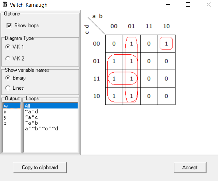
Also you can determine its expression from the Karnaugh map as shown below:
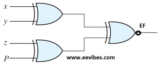
The circuit diagram for parity generator is shown in the figure below:
Even Parity Detector Circuit
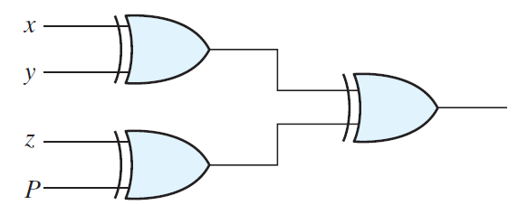
For the even parity detector, we need to have three inputs (x,y,z) along with the parity bit so that it could be deiced easily either there is some error or not. Since the information is transmitted with even parity so there must be even number of 1’s in the received message.
An error is occurred in the transmitted message if the received message has odd number of 1’s in it. This will indicate that one of the bits has changed its value.
Now, lets derive an expression for even parity detector circuit. The resulting function that models this behavior is named as error function. Its values are listed in the following table.
| w | y | z | P | Error Function (EF) |
| 0 | 0 | 0 | 0 | 0 |
| 0 | 0 | 0 | 1 | 1 |
| 0 | 0 | 1 | 0 | 1 |
| 0 | 0 | 1 | 1 | 0 |
| 0 | 1 | 0 | 0 | 1 |
| 0 | 1 | 0 | 1 | 0 |
| 0 | 1 | 1 | 0 | 0 |
| 0 | 1 | 1 | 1 | 1 |
| 1 | 0 | 0 | 0 | 1 |
| 1 | 0 | 0 | 1 | 0 |
| 1 | 0 | 1 | 0 | 0 |
| 1 | 0 | 1 | 1 | 1 |
| 1 | 1 | 0 | 0 | 0 |
| 1 | 1 | 0 | 1 | 1 |
| 1 | 1 | 1 | 0 | 1 |
| 1 | 1 | 1 | 1 | 0 |
If you look at the behavior of error function, it can be noticed that it produces output equal to 1 when there are odd number of 1’s are present at the input side including the parity bit. Hence again it is the XOR function behavior.
EF=x ⊕y ⊕z⊕P
As both even parity generator and detector circuits are implemented using XOR gates. So one interesting point is that we can use the same circuit at the transmitter and receiving side with the P bit grounded at the transmitting side.
How to design an Odd parity Generator and Detector Circuit?
Odd Parity Generator Truth Table and Circuit
Once you are clear about even parity generator and detector circuit, you can use the same idea for designing the odd parity generator and detector circuit. So, consider the above table again but now parity function will have value equal to 1 when there will be even number of 1’s in the input combination.
| x | y | z | P |
| 0 | 0 | 0 | 1 |
| 0 | 0 | 1 | 0 |
| 0 | 1 | 0 | 0 |
| 0 | 1 | 1 | 1 |
| 1 | 0 | 0 | 0 |
| 1 | 0 | 1 | 1 |
| 1 | 1 | 0 | 1 |
| 1 | 1 | 1 | 0 |
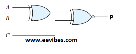
If you closely look at the parity function then it can be observed that the parity function is having value equal to 1 when there are even number of 1’s at the input side and its value is 0 when there are odd number of 1’s at the input side. This is actually the property of XNOR gate. So odd parity generator circuit can be implemented using 3-input XNOR gate.
P=(x ⊕y ⊕z)’
Odd Parity Detector Truth Table and Circuit
| w | y | z | P | Error Function (EF) |
| 0 | 0 | 0 | 0 | 1 |
| 0 | 0 | 0 | 1 | 0 |
| 0 | 0 | 1 | 0 | 0 |
| 0 | 0 | 1 | 1 | 1 |
| 0 | 1 | 0 | 0 | 0 |
| 0 | 1 | 0 | 1 | 1 |
| 0 | 1 | 1 | 0 | 1 |
| 0 | 1 | 1 | 1 | 0 |
| 1 | 0 | 0 | 0 | 0 |
| 1 | 0 | 0 | 1 | 1 |
| 1 | 0 | 1 | 0 | 1 |
| 1 | 0 | 1 | 1 | 0 |
| 1 | 1 | 0 | 0 | 1 |
| 1 | 1 | 0 | 1 | 0 |
| 1 | 1 | 1 | 0 | 0 |
| 1 | 1 | 1 | 1 | 1 |
EF=(x ⊕y ⊕z⊕P)’
Video Lecture for even and odd parity generator and detector circuit.
Design a four-bit combinational circuit 2’s complementer. (The output generates the 2’s complement of the input binary number.) Show that the circuit can be constructed with exclusive-OR gates. Can you predict what the output functions are for a five-bit 2’s complementer?
The first step of designing this combinational circuit involves the construction of truth table for the input variables a, b, c, d and output variables w, x, y, z.
For learning how to take the 2’s complement of a function watch this lecture:
The truth table for this problem is constructed below as:
|
Input |
Output |
||||||
| a | b | c | d | w | x | y | z |
|
0 |
0 | 0 | 0 | 0 | 0 | 0 | 0 |
|
0 |
0 | 0 | 1 | 1 | 1 | 1 |
1 |
|
0 |
0 | 1 | 0 | 1 | 1 | 1 |
0 |
|
0 |
0 | 1 | 1 | 1 | 1 | 0 | 1 |
|
0 |
1 | 0 | 0 | 1 | 1 | 0 |
0 |
| 0 | 1 | 0 | 1 | 1 | 0 | 1 |
1 |
|
0 |
1 | 1 | 0 | 1 | 0 | 1 | 0 |
| 0 | 1 | 1 | 1 | 1 | 0 | 0 |
1 |
|
1 |
0 | 0 | 0 | 1 | 0 | 0 | 0 |
| 1 | 0 | 0 | 1 | 0 | 1 | 1 |
1 |
|
1 |
0 | 1 | 0 | 0 | 1 | 1 | 0 |
| 1 | 0 | 1 | 1 | 0 | 1 | 0 |
1 |
|
1 |
1 | 0 | 0 | 0 | 1 | 0 | 0 |
| 1 | 1 | 0 | 1 | 0 | 0 | 1 |
1 |
|
1 |
1 | 1 | 0 | 0 | 0 | 1 | 0 |
| 1 | 1 | 1 | 1 | 0 | 0 | 0 |
1 |
The next step is to treat each output variable as an output function and derive its expression as a combination of a,b,c,d using k-map.
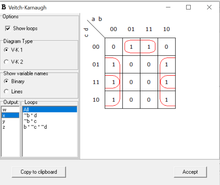
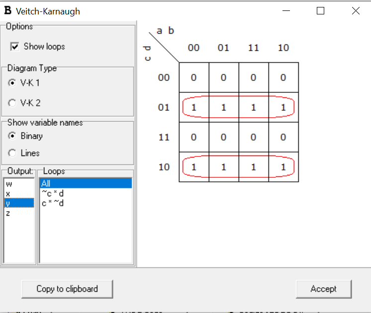
We can Write the output functions as:
w=[a⊕(b+c+d)]
x=[b⊕(c+d)]
y=[c⊕d]
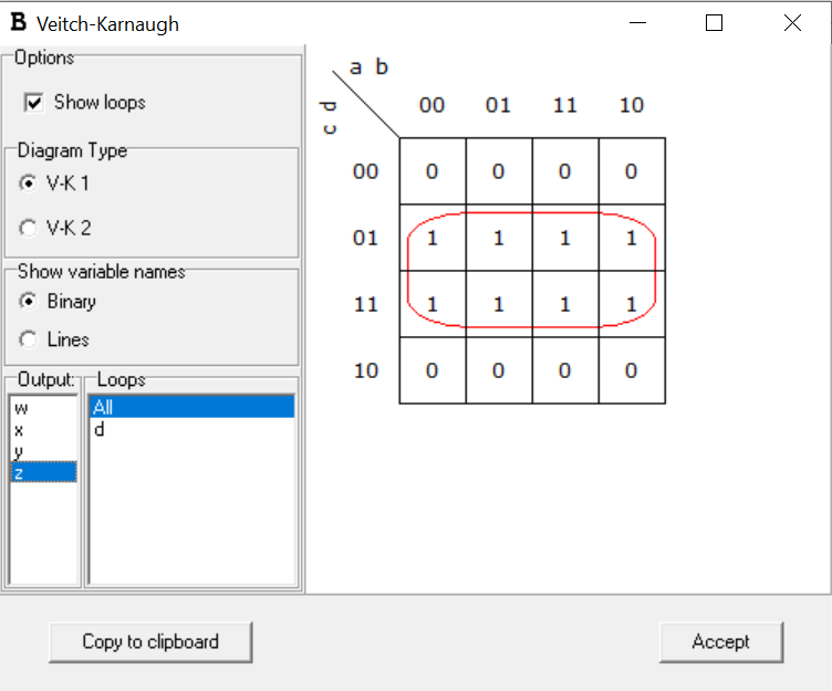
z=d
using the same approach, you can extend the idea to 5-input variables whose 2’s complement is desired.
v=[a⊕(b+c+d+e)]
w=[b⊕(c+d+e)]
x=[c⊕(d+e)]
y=[d⊕e]
z=d
Design a 4-bit Circuit that takes the 2’s Complement using XOR Gates
- What are the CMOS Logic Gates?
- What is the magnitude comparator circuit? Design a 3 bit magnitude comparator circuit
- What are the synchronous counters? Explain with an example.
- what are the half adder and full adder circuits?
- what are the half subtractor and full subtractor circuits?
- How to design a four bit adder-subtractor circuit?
- What are number systems in computer?
- Discuss the binary counter with parallel load? Explain its working with an example
- how to draw state diagram of sequential circuit?
- How to simplify a Boolean function using Karnaugh map (k-map)?
- What are the flip flops and registers in digital design?
- Define fan-in, fan-out, CMOS and TTL logic levels
- what is the Canonical form representation of Boolean function?
- What is difference between latches and flip flops?