Table of Contents
Introduction
How to Use the CAD Tools to Implement Circuits in CPLDs? The simplest way of describing a Complex Programmable Logic Device (CPLD) is to say that a CPLD consists of multiple SPLD-like blocks on a single chip. This statement is fairly accurate, but CPLDs are much more sophisticated than SPLDs, even at the level of their basic SPLD-like structures.
Using the AUTOCAD the burden on the designer is usually minimal, since the CAD tools are intended to be fully automatic. Circuit is arranged such that, in combination with the two logic gates, a very wide range of functions can be implemented in a single logic block. About half of the logic blocks also contain a flip-flop.
Steps Involved for Implementing Circuits in CPLDs
The steps involved for implementing circuits in CPLDs are mostly the same as for SPLDs, but the tools themselves are more refined. Because the devices are complex and can accommodate large designs, commonly a mixture of design entry methods is used for different modules of a complete circuit. For instance, some modules might be designed with a small hardware description language like ABEL, others drawn using a symbolic schematic capture tool, and still others described via a full-featured hardware description language such as VHDL.
This implies that for CPLDs an especially important step in the CAD system is the merging of pieces of a design into a single large circuit and then “fitting” that circuit into the CPLD. Because of the complexity involved, this task of mapping a circuit into the device must be performed automatically by sophisticated CAD programs, which are supplied either by the CPLD manufacturer or a third party. the maximum size of circuit that will fit in the largest available CPLDs is about 5000 gates.
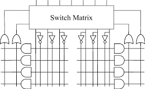
The CPLD structure is shown in the above figure.
All the CPLDs share common features and offer similar capabilities; they differ mostly in the way in which their features are implemented, such as with larger or smaller AND- and OR- planes, different numbers of flip-flops configurable in various ways, a range of maximum logic capacities, different programming technologies (fuses, EPROM, EEPROM), varying numbers of interconnect wires, in-circuit versus out-of-circuit programmability, and others.
In terms of software CAD tool design cycles, typical steps performed for SPLDs include: initial design entry, logic optimization, device fitting, simulation, and configuration. This design flow is illustrated in Fig. below, which also indicates how some stages feedback to others. Referring to the figure, design entry may be done either by creating a schematic diagram with a graphical CAD tool or by using a text-based system to describe a design in a simple hardware description language.
It is also possible for sections of a design to be created in different ways and then translate and merge the pieces into a complete circuit, but this is normally done only for larger designs. Since initial logic entry is not usually in an optimal form, CAD tools are employed to optimize the circuits, after which additional programs analyze the resulting logic equations and “fit” them into the SPLD. Simulation is used to verify correct operation, and the user would go back to design entry to fix errors. When a design simulates correctly it can be loaded into a programming unit and an SPLD configured.
CPLD Applications
- Their high speeds and wide range of capacities make CPLDs useful for many applications, from implementing random glue logic to prototyping small gate arrays.
- An important reason for the growth of the CPLD market is the conversion of designs that consist of multiple SPLDs into a smaller number of CPLDs.
- CPLDs can realize complex designs such as graphics, LAN, and cache controllers. As a rule of thumb, circuits that are exploit wide AND/OR gates and do not need a large number of flip-flops are good candidates for CPLD implementation.
- Finite state machines are an excellent example of this class of circuits. A significant advantage of CPLDs is that they allow simple design changes through reprogramming (all commercial CPLD products are reprogrammable).
- In-system programmable CPLDs even make it possible to reconfigure hardware (for example, change a protocol for a communications circuit) without powering down.
- Designs often partition naturally into the SPLD-like blocks in a CPLD, producing more predictable speed performance than a design split into many small pieces mapped into different areas of the chip.
- Predictability of circuit implementation is one of the strongest advantages of CPLD architectures.
Also read here
- Explain the FSM as an Arbiter Circuit in Details?
- Discuss the Several System Design Examples using ASM Charts Clock
- What are the Techniques for Testing Digital Circuits?
- What are Arithmetic Comparison Circuits? Explain with examples.
- How to Design Combinational Logic Circuits by using Metaheuristic Algorithm?
- What are the Transmission Gates?
- What are number systems in computer?
- Number System Conversions – Briefly Explained
- How to design Half adder and Full adder circuits?
- What are the decoders? how are they different from encoders?
- What is binary arithmetic? How to add, subtract, multiply and divide two binary numbers?
- What is the magnitude comparator circuit? Design a 3 bit magnitude comparator circuit
- How to design a 4 bit magnitude comparator circuit?
- How many hundreds are there in 1000?
- What are the synchronous counters? Explain with an example
- what are the BCD and binary ripple counters?