Introduction
What are the Power Efficient XOR and XNOR Gates? The advancement of Gates technology has set down the Plan of Universal logic gates at substantial ranks of abstraction with studies up to Gates. Realizing that circuits for low power and small area have become an important issue with the development of integrated circuits in the direction of very high integrated density and high operating frequency the area includes the number of transistors and the power supply requirements. With the reduction of the technology node, the power supply requirement is also reduced to a greater extent so the logic design with low power supply becomes a necessity of time. Power consumption can be minimized by minimizing the supply voltage Designers can achieve low power consumption but must balance other requirements such as speed and reliability.
Ease of Usage
Many designs have been reported to realize XOR functions using a number of different circuit techniques and approaches. They differ in the methodology and number of transistors to improve the performance of the circuit in terms of speed and density, Low power consumption is one of the key design criteria for all IC designers at all design levels, along with latency and area considerations.
Applications
XOR gates have many applications in electronic circuits. It is used in simple digital adder circuits to calculate the sum and carry of two (half adder) or three bit numbers (full adder).
XOR Gate with Transistors
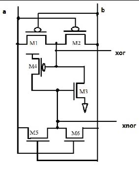
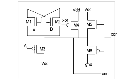
Low power XOR/XNOR logic can be designed with different logic patterns as specified with reduced VDD, low operating frequency and less switching operation Here we design an XOR and XNOR In this circuit design, two cross-coupled circuits are connected by feedback technique using PMOS transistor and NMOS transistor, The VDD of this circuit can vary from 0.6V to 3.3V. The cross-coupled NMOS produces a “high” logic level at its output when both “a” and “b” inputs are “high”. Therefore, trigger signal is used to pass a “low” logic level to the output of the XOR signal. Similarly, a cross-coupled PMOS produces a ‘low’ logic level at the output when ‘a’ and ‘b’ inputs are ‘low’ and using a trigger signal, which can produce a logic level ‘high’ to XNOR output.
Logic Expression
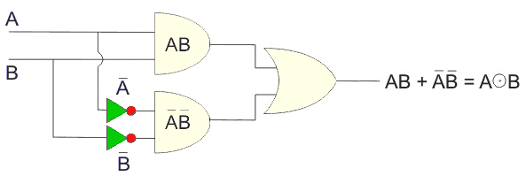
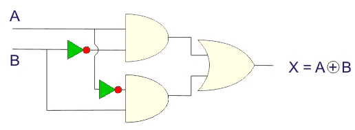
The XOR and XNOR gate function are denoted by ⊕ and dot in circle respectively. The logic expression for XOR and XNOR are
XNOR Gate
Truth Table:
| A | B | XOR | XNOR |
| 0 | 0 | 0 | 1 |
| 0 | 1 | 1 | 0 |
| 1 | 0 | 1 | 0 |
| 1 | 1 | 0 | 1 |
Proposed Design:
The proposed XOR-XNOR gate design using six transistors is shown in the figure. It uses a through-transistor and CMOS inverter concept. The inverter is used as a drive output so that the achieves perfect output performance. Connect Vdd to transistors M3 and M4 used to drive a good output of ‘1’. Transistor M4 is used to drive output signal when XOR output ‘0’ when input signal A = B = 1. In this condition, when transistor M1 or M2 is turned on, it will outputs a bad ‘1’ signal to input of the inverter The XOR output will also be attenuated and to get a good output the transistor M4 is ON when the Xor output is ‘0’ then it will perfectly transfer the ‘1’ signal from Vdd to the XOR output.
Also read here:
- How to Draw State Diagram of Sequential Circuit?
-
How to design a 4 bit magnitude comparator circuit? Explanation with examples
-
What is the magnitude comparator circuit? Design a 3 bit magnitude comparator circuit
-
What are the synchronous counters? Explain with an example.
-
what are the half adder and full adder circuits?
-
what are the half subtractor and full subtractor circuits?
-
How to design a four bit adder-subtractor circuit?
-
What are number systems in computer?
-
Discuss the binary counter with parallel load? Explain its working with an example
-
how to draw state diagram of sequential circuit?
-
How to simplify a Boolean function using Karnaugh map (k-map)?
-
What are the flip flops and registers in digital design?
-
Define fan-in, fan-out, CMOS and TTL logic levels
-
what is the Canonical form representation of Boolean function?
-
What is difference between latches and flip flops?